Drive power amplifier with adjustable gain of 0.1-3GHz CMOS

A technology for power amplifiers and power amplifier circuits, which is applied in the field of ultra-wideband CMOS gain-adjustable drive power amplifiers, and can solve the difficulties of input and output matching circuits, the difficulty of adjustable gain flatness, and the difficulty of ultra-wideband input matching, etc. problem, to achieve the effect of improving ultra-wideband matching characteristics, avoiding low breakdown voltage characteristics, good broadband characteristics and gain flatness

Inactive Publication Date: 2014-04-23
TIANJIN UNIV
View PDF2 Cites 10 Cited by
  • Summary
  • Abstract
  • Description
  • Claims
  • Application Information

AI Technical Summary

Problems solved by technology

However, the traditional single-stage stacking structure based on CMOS technology has the following problems: 1) low power gain 2) very difficult to match ultra-wideband input 3) serious loss of high-frequency gain
[0010] 1. The chip area of

Method used


Image

  • Drive power amplifier with adjustable gain of 0.1-3GHz CMOS
  • Drive power amplifier with adjustable gain of 0.1-3GHz CMOS

Examples


Embodiment Construction

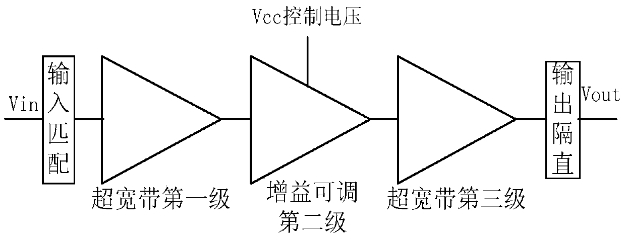
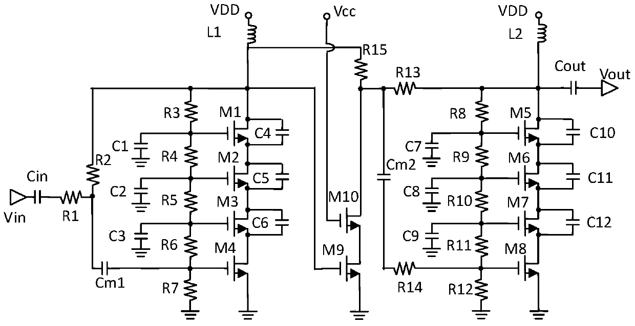
[0022] The 0.1-3GHz CMOS gain-adjustable drive power amplifier of the present invention is a three-stage gain-adjustable four-stage stack structure capacitor compensation amplifier, which is designed by CMOS technology.

[0023] It includes an input matching circuit, an ultra-wideband driver amplifier circuit, an adjustable gain amplifier circuit, an ultra-wideband power amplifier circuit and an output DC blocking circuit. It is an active two-port amplifying network; the input matching circuit is composed of an off-chip DC blocking capacitor at the input end, a matching resistor, a feedback resistor and a DC blocking coupling capacitor; the output DC blocking circuit is composed of a DC blocking coupling capacitor.

[0024] Among them, the first stage of the circuit is an ultra-wideband driving stage, which is used to realize the ultra-wideband driving power gain of its amplifier and ensure the matching of the ultra-wideband S11 parameters of the entire circuit; the second stag...


PUM


Abstract

The invention discloses a drive power amplifier with the adjustable gain of a 0.1-3GHz CMOS. The drive power amplifier comprises an input match circuit, an ultra-wideband drive stage amplifying circuit, a gain-adjustable amplifying circuit, an ultra-wideband power amplifying circuit and an output blocking circuit. A first ultra-wideband drive stage is used for achieving preceding-stage gain and ensuring ultra-wideband input match of the whole circuit. A gain control circuit is used for controlling power gain of wideband radio frequency signals and the good inter-ultra-wideband matching property. A third ultra-wideband drive power stage is used for ensuring large power output of the whole circuit and the good wideband output matching property. A three-stage stacking structure is combined with a compensation capacitance circuit, and the area of a chip is small. In the whole circuit, parameters of an adopted component can be determined according to indexes of items such as the whole circuit gain, the wideband and the output power, and therefore the adjustable gain, the high-linearity and the high drive power within the 0.1-3GHz can be achieved.

Description

technical field [0001] The invention relates to the field of complementary metal-oxide-semiconductor (CMOS) radio frequency power amplifiers and integrated circuits, in particular to an ultra-wideband CMOS gain-adjustable drive power amplifier covering the application of industry-specific network frequency bands. Background technique [0002] The rapid development of wireless communication markets such as mobile phones, cordless phones, radio frequency tags (RFID), and wireless local area networks (WLAN) has continuously promoted the development of RF front-end transceivers in the direction of high integration, low power consumption, compact structure, and low price. More and more single-chip radio frequency transceiver communication systems are designed and implemented using cheap and relatively mature and reliable CMOS technology, which requires more and more communication system sub-modules to be designed with CMOS technology while ensuring high performance, so that A hig...

Claims


Application Information

Patent Timeline
IPC IPC(8): H03F3/189H03F3/20H03G3/20H03F1/42
Inventor 马建国邬海峰王立果周鹏王建利
Owner TIANJIN UNIV
Why Eureka
Try Eureka