
Circuit substrate and preparation method thereof

A circuit substrate, electronic-level technology, applied in circuit substrate materials, printed circuit manufacturing, printed circuits, etc., can solve the problem of not considering signal delay and other issues

Active Publication Date: 2014-04-30
GUANGDONG SHENGYI SCI TECH
View PDF7 Cites 37 Cited by
  • Summary
  • Abstract
  • Description
  • Claims
  • Application Information

AI Technical Summary

Problems solved by technology

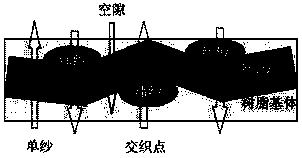
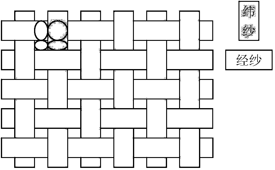
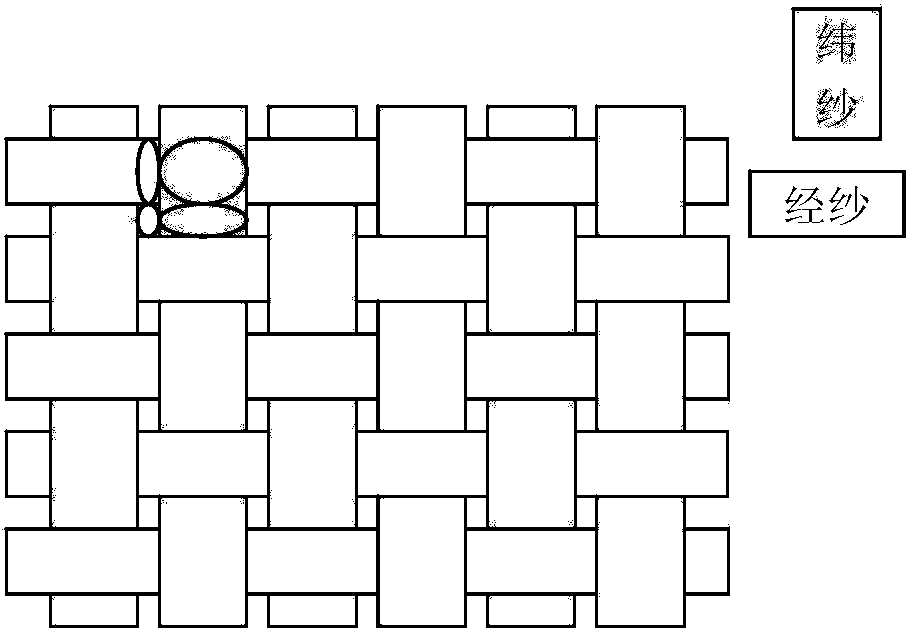
[0024] None of the above considers or proposes to solve the problem of signal delay in the plane direction of the circuit substrate, that is, the warp and weft directions, simply and conveniently in the conventional production process.

Method used


Image

  • Circuit substrate and preparation method thereof
  • Circuit substrate and preparation method thereof
  • Circuit substrate and preparation method thereof

Examples


Embodiment 1

[0096] Use E-type 1080 glass fiber cloth (mass per unit area is 46.8g / m 2 ) as a reinforcing material, the epoxy resin composition was dissolved in a solvent and then added with a filler as a pretreatment glue. Table 1 shows the composition of the glue formula and the physical properties of the circuit board. The steps for making the circuit board are as follows:

[0097] Step 1: Prepare pretreatment glue. Take a suitable container, add 40 parts by mass of epoxy resin composition, an appropriate amount of butanone solvent, stir for a certain period of time, then add 52 parts by mass of rutile titanium dioxide filler and 8 parts by mass of amorphous silica filler, and carry out Stir well, and emulsify and disperse to form the pretreatment glue. The Dk of the glue is 6.6.

[0098] Step 2: Prepare pretreated E-type glass fiber cloth. Use the above pretreatment glue to pre-impregnate the E-type glass fiber cloth, and dry the solvent after completion to obtain a pretreated glass...

Embodiment 2

[0102] Use E-type 1080 glass fiber cloth (mass per unit area is 46.8g / m 2 ) as a reinforcing material, the epoxy resin composition was dissolved in a solvent and then added with a filler as a pretreatment glue. Table 1 shows the composition of the glue formula and the physical properties of the circuit board. The steps for making the circuit board are as follows:

[0103] Step 1: Prepare pretreatment glue. Take a suitable container, add 42 parts by mass of epoxy resin composition, an appropriate amount of butanone solvent, stir for a certain period of time, then add 50 parts by mass of rutile titanium dioxide filler and 8 parts by mass of amorphous silica filler, and carry out Stir well, and emulsify and disperse to form the pretreatment glue, the glue Dk is 6.5.

[0104] Step 2: Prepare pretreated E-type glass fiber cloth. Use the above pretreatment glue to pre-impregnate the E-type glass fiber cloth, and dry the solvent after completion to obtain a pretreated glass fiber ...

Embodiment 3

[0108] Use E-type 1080 glass fiber cloth (mass per unit area is 46.8g / m 2 ) as a reinforcing material, the cyanate resin composition was dissolved in a solvent and then added with fillers as a pretreatment glue, the composition of the glue formula and the physical property data of the circuit board are shown in Table 1. The steps for making the circuit board are as follows:

[0109] Step 1: Prepare pretreatment glue. Take a suitable container, add 40 parts by mass of cyanate resin composition, an appropriate amount of butanone solvent, stir for a certain period of time, then add 54 parts by mass of rutile titanium dioxide filler and 6 parts by mass of amorphous silica filler, Thoroughly stir, emulsify and disperse to form the pretreatment glue, and the Dk of the glue is 6.5.

[0110] Step 2: Prepare pretreated E-type glass fiber cloth. Use the above pretreatment glue to pre-impregnate the E-type glass fiber cloth, and dry the solvent after completion to obtain a pretreated ...


PUM


Abstract

The invention provides a preparation method of a bonding sheet forming a circuit substrate. The method comprises a step of pretreating a glass fabric by use of a pretreatment glue solution of which the dielectric constant (Dk) is the same with or close to the Dk value of the adopted glass fabric. The invention also provides a bonding sheet and a circuit substrate prepared by the method. The preparation method of the circuit substrate provided by the invention does not need equipment transformation and adjustment, the cost is relatively low, the difference of the dielectric constant of the prepared circuit substrate in the longitudinal direction and latitudinal direction is less, and the problem of signal delay can be effectively solved.

Description

technical field [0001] The invention belongs to the technical field of electronic materials, and relates to a circuit substrate and a manufacturing method thereof, in particular to a circuit substrate with microscopic uniformity and isotropy and a manufacturing method thereof, and more specifically to a dielectric constant in the warp direction. A circuit substrate with little difference from the weft direction and a manufacturing method thereof. Background technique [0002] In recent years, with the development of electronic products in the direction of multi-function and miniaturization, the circuit boards used are developing in the direction of multi-layer, high-density wiring and high-speed signal transmission. , such as the comprehensive performance of copper clad laminates put forward higher requirements. Specifically, the dielectric constant (Dk) and dielectric loss (Df) of the medium are important indicators that affect the signal transmission speed and signal qual...

Claims


Application Information

Patent Timeline
Patent Type & Authority Applications(China)
IPC IPC(8): C08J5/24C08J5/06C08L63/00C08L79/04C08L71/12C08L47/00C09J7/00B32B15/08B32B27/04H05K1/03
CPCC08J2323/20C08J2363/00C08J2371/12C08J2379/04H05K2201/029H05K1/0366C08J5/248C03C25/16C03C25/30C03C25/326C03C25/36H05K1/0306H05K1/0393H05K3/0011H05K3/0085
Inventor 颜善银曾宪平许永静杨中强苏晓声罗俐
Owner GUANGDONG SHENGYI SCI TECH
Learn More