Bigrid optoelectronic thin film transistor, pixel circuit and pixel array

A technology for optoelectronic thin films and pixel circuits, applied in transistors, circuits, and electrical solid-state devices, etc., can solve the problems of low integration, poor pixel performance, and complex manufacturing processes.

Active Publication Date: 2014-04-30
广州爱瑞玥芯科技有限公司
View PDF3 Cites 48 Cited by
  • Summary
  • Abstract
  • Description
  • Claims
  • Application Information

AI Technical Summary

Problems solved by technology

[0010] In the detection pixel unit mentioned above, the components responsible for visible light detection (such as photosensitive diode, MSM photoconductive or photoelectric thin film transistor) are sepa

Method used


Image

  • Bigrid optoelectronic thin film transistor, pixel circuit and pixel array
  • Bigrid optoelectronic thin film transistor, pixel circuit and pixel array
  • Bigrid optoelectronic thin film transistor, pixel circuit and pixel array

Examples


Embodiment Construction

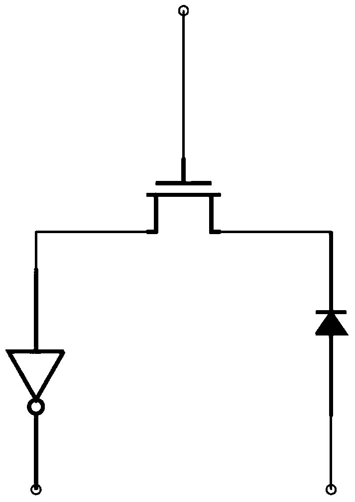
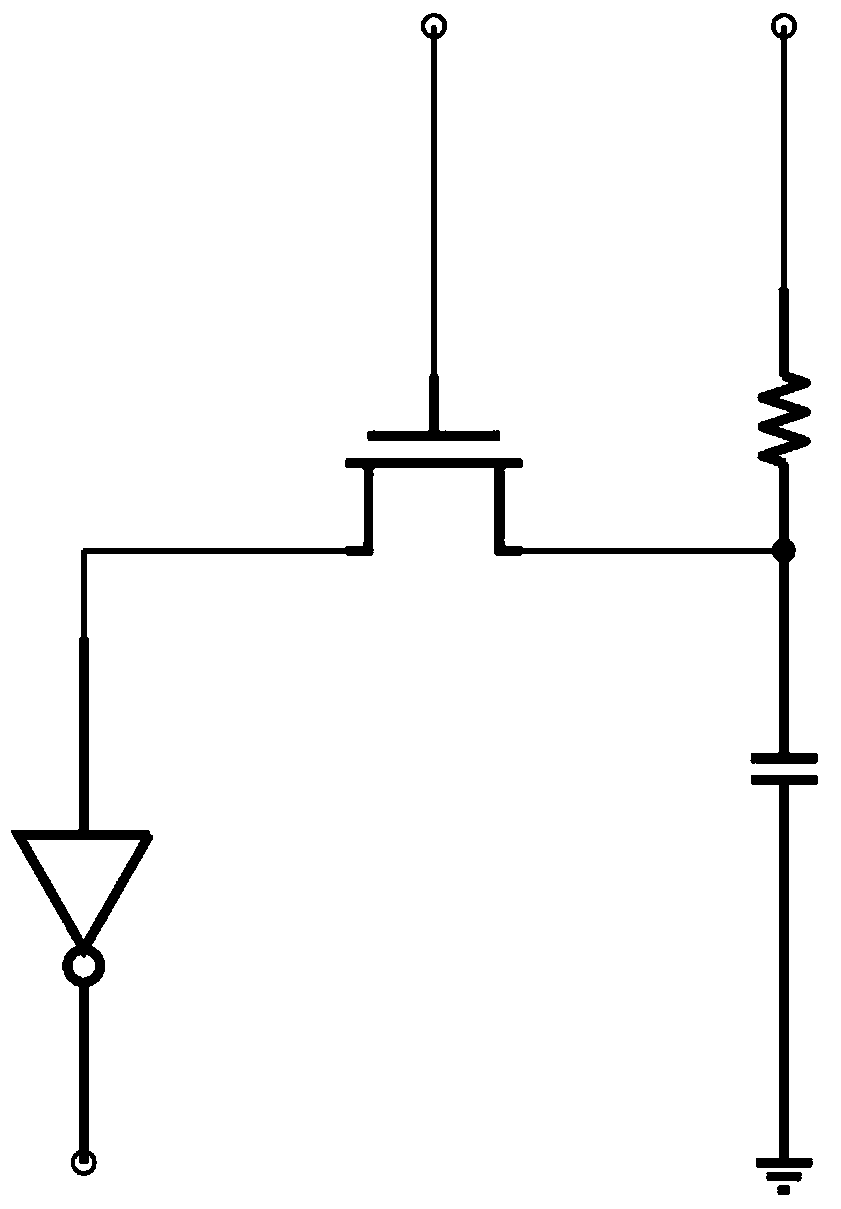
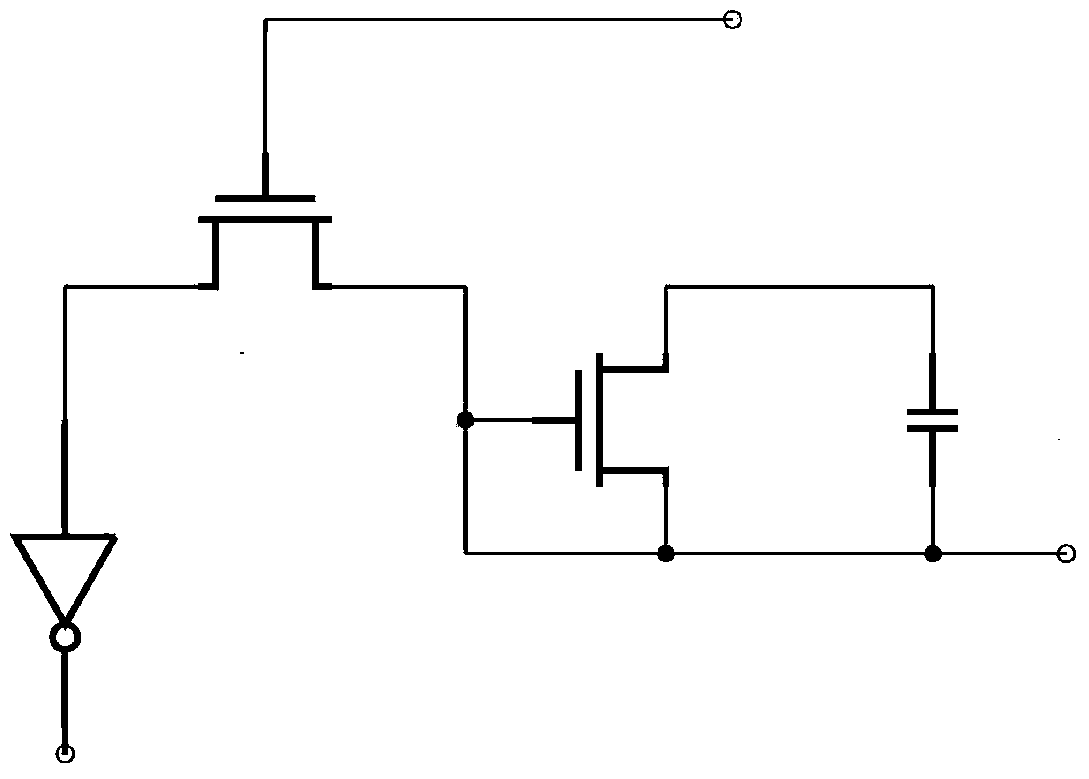
[0042] see Figure 4 , which is one of the cross-sectional structure diagrams of a double-gate photoelectric thin film transistor of the present invention. The double-gate photoelectric thin film transistor includes a substrate 1 , a dark gate 2 , a first dielectric layer 3 , a source 4 , a drain 5 , a channel layer 6 , a second dielectric layer 7 and a light gate 8 . The substrate 1 can be a glass substrate, a plastic substrate or other substrates; in the present invention, a glass substrate is used. The dark gate 2 is disposed on the substrate 1 and is made of metal or metal alloy, such as molybdenum, chromium or aluminum or their alloys. The first dielectric layer 3 is disposed on the substrate 1 and covers the dark gate 2 . The source 4 and the drain 5 are disposed on the first dielectric layer 3 and are in contact with both ends of the first dielectric layer 3 correspondingly; the channel layer 6 is disposed on the first dielectric layer 3 and cover the source 4 and th...


PUM

PropertyMeasurementUnit
Thicknessaaaaaaaaaa

Abstract

The invention provides a bigrid optoelectronic thin film transistor capable of being used for indirect detecting type digital X-ray detectors. In pixel units for indirect X-ray detecting, optoelectronic detecting elements and thin film transistors for signal reading are integrated in the bigrid optoelectronic thin film transistor. The bigrid optoelectronic thin film transistor can achieve the on-off and signal amplification performance of the thin film transistors, and can also achieve the induction function of optoelectronic transistors and the storage function of signal charges. According to the scheme, the bigrid optoelectronic thin film transistor has the advantages of being high in signal to noise ratio and resolution ratio, simple in manufacturing technique and high in integrity degree, pixel areas can be utilized fully, and high-sensitivity detection can be achieved.

Description

technical field [0001] The invention relates to a structure, a preparation process and a pixel circuit of a double gate photoelectric thin film transistor. Background technique [0002] X-ray imaging is one of the most commonly used diagnostic techniques in hospitals. Such as chest X-ray, mammary X-ray, blood vessel instrument and gastrointestinal instrument, etc. have been widely used in medical practice and become an important tool to help doctors diagnose patients. In recent years, the development of flat-panel display technology has led to the vigorous development of flat-panel X-ray imaging technology for biomedical imaging, which has constituted an important branch of biomedical imaging. At present, digital flat-panel X-ray imagers have been put into the market and become a strong competitor of traditional X-ray imaging technology. Its outstanding advantages lie in digitization, high sensitivity and high resolution, etc. These advantages have played an important rol...

Claims


Application Information

Patent Timeline
IPC IPC(8): H01L31/0224H01L27/146
CPCH01L27/14612H01L27/14658H01L31/022408
Inventor 王凯陈军欧海
Owner 广州爱瑞玥芯科技有限公司
Why Eureka
Try Eureka