Wafer temporary bonding method

A technology of temporary bonding and temporary bonding glue, which is applied in the manufacturing of electrical components, electrical solid-state devices, semiconductor/solid-state devices, etc. Affect device performance and other issues to prevent slippage and offset, increase contact area, and reduce production costs

Active Publication Date: 2014-05-14
TSINGHUA UNIV
View PDF5 Cites 3 Cited by
  • Summary
  • Abstract
  • Description
  • Claims
  • Application Information

AI Technical Summary

Problems solved by technology

[0003] However, the above-mentioned temporary bonding adhesive has the following two problems: one is that when the wafer and the supporting sheet are temporarily bonded, the temporary bonding adhesive softens due to the high bonding temperature, which finally causes a certain degree of friction between the wafer and the supporting sheet. Sliding offset, which can easily lead to wafer edge cracking during the subsequent thinning process; the second problem is that when the thinned wafer is bump-bonded with other wafers, due to the temporary bonding glue The fluidity of the bumps leads to a certain displacement deviation between the bumps and the bonding between the bumps, which affects the performance of the device
Therefore, it is difficult to continue using the temporary bonded sheet

Method used


Image

  • Wafer temporary bonding method
  • Wafer temporary bonding method
  • Wafer temporary bonding method

Examples


Embodiment Construction

[0024] The following will clearly and completely describe the technical solutions in the embodiments of the present invention with reference to the drawings in the embodiments of the present invention. Apparently, the described embodiments are only some of the embodiments of the present invention, but not all of them. Based on the embodiments of the present invention, all other embodiments obtained by persons of ordinary skill in the art without making creative efforts belong to the protection scope of the present invention.

[0025] Secondly, the present invention is described in detail with reference to the schematic diagrams. When describing the embodiments of the present invention in detail, for the convenience of explanation, the schematic diagrams are only examples, which should not limit the protection scope of the present invention.

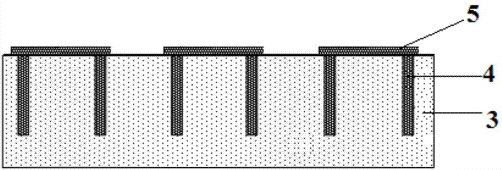
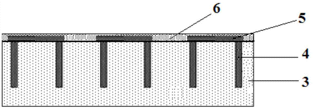
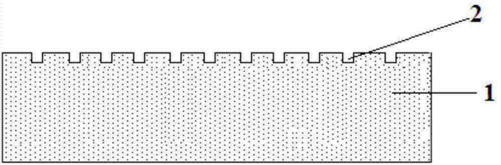
[0026] The invention provides a wafer temporary bonding method, which comprises: roughening the surface of a supporting sheet; bonding t...


PUM


Abstract

The invention discloses a wafer temporary bonding method. The method includes the steps that a silicon through hole and front face manufacturing technology of a wafer is completed; the front face of the wafer is coated with temporary bonding glue; the surface of a supporting piece is roughened; the roughened surface of the supporting piece is bonded with the front face, coated with the temporary bonding glue, of the wafer; the back face of the wafer bonded with the supporting piece is thinned until the thickness of the wafer reaches a needed value; a back face manufacturing technology of the wafer after the back face is thinned is finished; the temporary bonding glue on the wafer after the back face manufacturing technology is removed. According to the method, due to the fact that the surface of the supporting piece is roughened, the contact area between the temporary bonding glue and the supporting piece is increased, and the temporary bonding glue is nested and fixed and prevented from sliding and offsetting at high temperature.

Description

technical field [0001] The invention relates to the field of semiconductor manufacturing, in particular to a wafer temporary bonding method. Background technique [0002] In the semiconductor three-dimensional integration technology, in order to meet the requirements of the device, it is necessary to thin the silicon wafer to a certain thickness to realize the upper and lower interconnection of through-silicon vias (TSVs). The manufacturing method of TSV structure generally includes the following steps: (1) deep hole etching of TSV, that is, TSV with high aspect ratio structure prepared by DRIE (deep reactive ion etching) process; (2) deep hole plating of TSV, that is TSVs are filled by sequentially depositing an insulating layer, a diffusion barrier layer and a seed layer on the sidewall of the deep hole; (3) Front side preparation process, that is, forming wiring and related devices on the front side of the wafer, in which according to the actual Process requirements, CMO...

Claims


Application Information

Patent Timeline
Patent Type & Authority Applications(China)
IPC IPC(8): H01L21/60
CPCH01L21/02H01L21/6835H01L2221/68327
Inventor 蔡坚魏体伟王谦
Owner TSINGHUA UNIV
Why Eureka
Try Eureka