
Heterogeneous photovoltaic solder strip and manufacturing method thereof

A photovoltaic ribbon and heterogeneous technology, which is applied in photovoltaic power generation, final product manufacturing, sustainable manufacturing/processing, etc., can solve the problems of overall electrical conductivity reduction of ribbon, waste of protective baseband 1, and increased fragmentation rate, etc., to achieve reduction Overall material cost, increase overall conductivity, and increase the effect of actual power

Inactive Publication Date: 2014-05-14
FUNDANT CHANGZHOU ADVANCED METAL TECH
View PDF5 Cites 10 Cited by
  • Summary
  • Abstract
  • Description
  • Claims
  • Application Information

AI Technical Summary

Problems solved by technology

For the first surface 3, the solder layer 2 is somewhat wasteful for protecting the base tape 1, and the first surface 3 causes the overall thickness of the solder tape to be thicker, which increases the fragmentation rate of the photovoltaic cell during welding and lamination, and the solder tape. The overall conductivity is reduced, which affects the power of photovoltaic cell modules

Method used

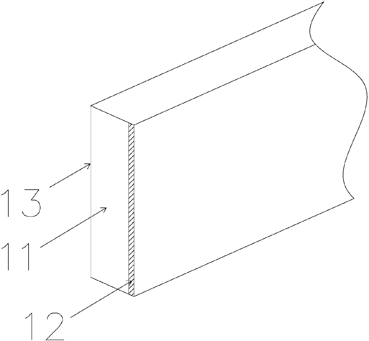
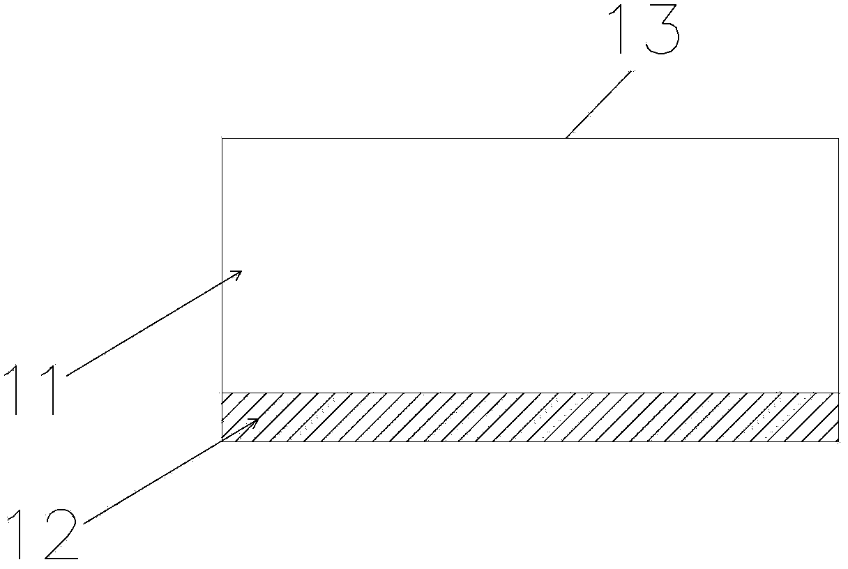
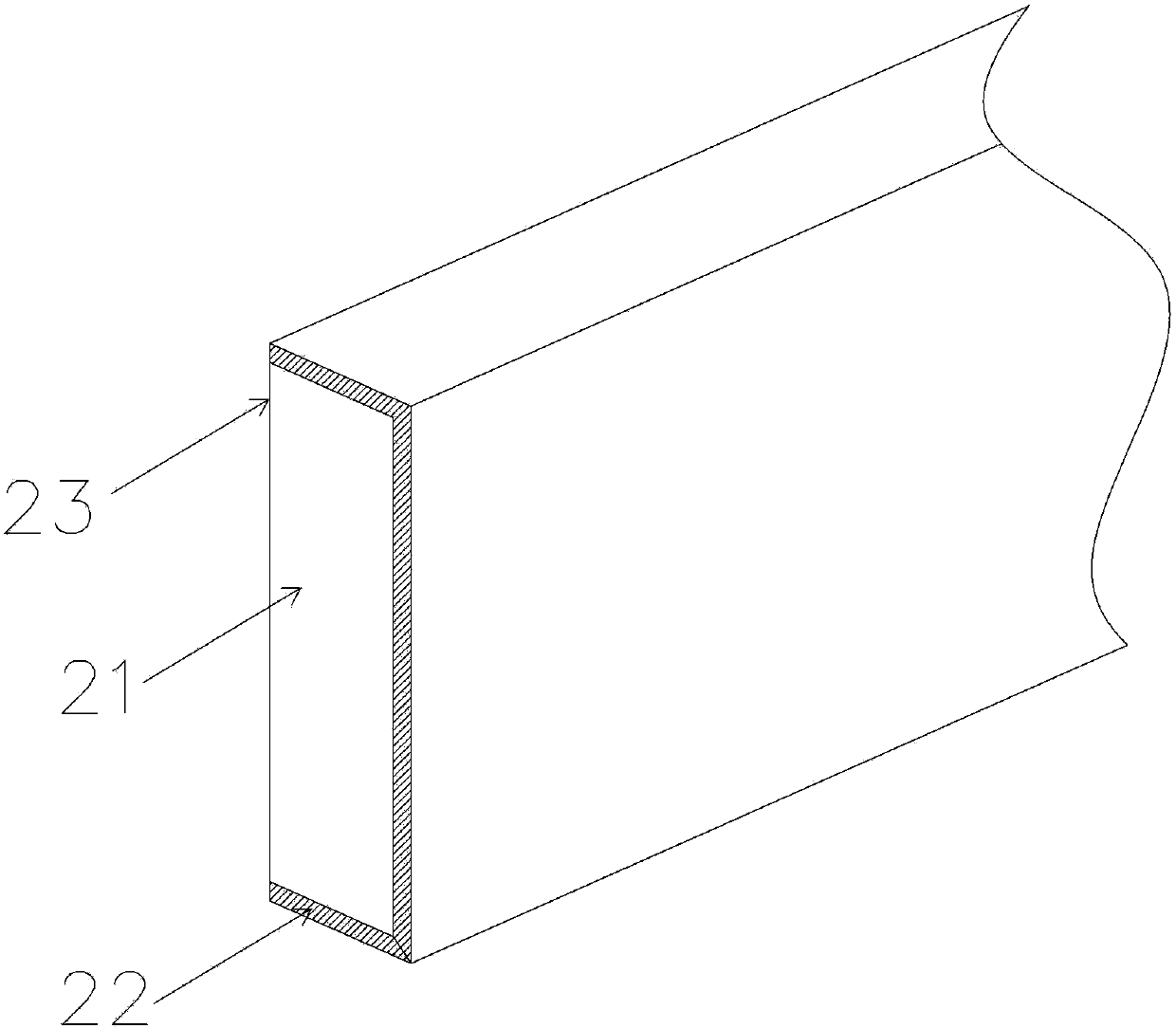

Image

  • Heterogeneous photovoltaic solder strip and manufacturing method thereof
  • Heterogeneous photovoltaic solder strip and manufacturing method thereof
  • Heterogeneous photovoltaic solder strip and manufacturing method thereof

Examples


Embodiment 1

[0035] This embodiment uses a wide-width oxygen-free copper (a kind of pure copper) base belt. After tempering, firstly, a wide surface of the base belt 11 is covered with waterproof stickers, or other materials with certain strength and reasonable dimension stability can also be used. permanent waterproof protective film. Afterwards, the base belt 11 is electroplated through the electroplating tank by pulling the waterproof self-adhesive. The electroplating solution used in this embodiment is a pure tin plating solution. One side of the waterproof self-adhesive base tape is covered with a layer of about 8 μm pure tin solder layer, and then the waterproof self-adhesive is removed to obtain a wide-width heterogeneous photovoltaic ribbon. Then through the slitting machine, the wide-width heterogeneous photovoltaic ribbon is slit into the required size ribbon with a width of 1.5 mm, and the wide surface not covered with solder is passivated and protected by pure copper passivatio...

Embodiment 2

[0039] In this embodiment, high-purity raw copper containing a certain proportion of lanthanum is used as the wide-width baseband. After tempering, the wide-width baseband is slit (or rolled) into the required size of 1.48 mm wide, and the slitted baseband 21 is a wide surface. Adhered to waterproof stickers, or other waterproof protective films with certain strength and reasonable dimensional stability. Then by pulling the waterproof sticker, the base belt 21 is electroplated through the electroplating tank. The electroplating solution used in this embodiment is a tin-copper plating solution. One side of the self-adhesive base tape is covered with a 10μm tin-copper solder layer, and then the waterproof self-adhesive is removed, and the non-solder surface is passivated to obtain the required size of the heterogeneous photovoltaic ribbon. prepared in photovoltaic modules.

[0040] Using 72 pieces of 156*156 polysilicon wafers, using this ribbon to prepare a set of battery modu...

Embodiment 3

[0043] In this embodiment, copper-aluminum alloy is used as the wide-width base tape. After tempering, the wide-width base tape is cut (or rolled) into the required size of 1.60 mm wide, and then a layer of 0.5 μm nickel protective film is pre-coated. One wide side of the cut base tape 31 containing the ultra-thin protective film 32 is adhered to the waterproof sticker, or it can be other waterproof protective film with certain strength and reasonable dimensional stability. Then, the base belt 31 is electroplated through the electroplating tank by pulling the waterproof self-adhesive. The electroplating solution first used in this embodiment is a tin-bismuth alloy plating solution. One side of the base tape 31 without waterproof self-adhesive is covered with a layer of 6 μm tin-bismuth solder layer 33, and then a pure tin plating solution is used. The solder layer is covered with a layer of 4 μm pure tin solder layer 34 and then the waterproof adhesive is removed, so as to obt...


PUM

PropertyMeasurementUnit
Thicknessaaaaaaaaaa
Thicknessaaaaaaaaaa

Abstract

The invention provides a heterogeneous photovoltaic solder strip and a manufacturing method thereof. Through an electroplating technology, electrotinning or tin alloy is performed on high conductive metal or an alloy base band. Under the condition that solderability is not reduced, a soldering tin layer on a non-soldering surface is removed. A thickness of the soldering tin layer of a soldering surface can be greatly reduced compared to the solder strip made through a traditional hot dip soldering mode. The non-soldering surface carries out base band surface passivation treatment or be served as an electroplating ultrathin protection film. Under an allowable solder-strip mechanical property, a thickness of a high conductivity matrix is maximized so that an overall conductivity of the solder strip is increased; battery pack power is increased because of an increase of solder strip conflux efficiency and simultaneously total material cost of the solder strip is reduced.

Description

technical field [0001] The invention belongs to the technical field of photovoltaic ribbon processing, and in particular relates to a heterogeneous photovoltaic ribbon and a preparation method thereof. Background technique [0002] With the rapid development of the world economy, energy consumption is increasing, and all countries in the world need the application and popularization of new energy. As the greenhouse gas effect caused by carbon dioxide emissions causes global warming and causes natural disasters, the demand for clean and renewable energy is particularly strong in countries around the world. Since the global crisis caused by the subprime mortgage crisis in the United States in 2007 has spread and expanded, in order to stimulate economic growth, countries have adopted more active measures to encourage the use of renewable energy. The Obama administration of the United States proposed to invest 150 billion US dollars in clean energy in the next 10 years; the Eur...

Claims


Application Information

Patent Timeline
IPC IPC(8): H01L31/05H01L31/02H01L31/18
CPCH01L31/0508H01L31/0512Y02E10/50Y02P70/50
Inventor 钱海鹏
Owner FUNDANT CHANGZHOU ADVANCED METAL TECH
Learn More