Surface incidence graphene photoelectric detector based on one-dimensional optical grating

A photodetector, graphene technology, applied in circuits, electrical components, semiconductor devices, etc., can solve the problem of the photodetector is not very clear, to improve the photocurrent generation efficiency, facilitate mass production, and improve the response speed. Effect

Active Publication Date: 2014-05-21
INST OF SEMICONDUCTORS - CHINESE ACAD OF SCI
View PDF6 Cites 30 Cited by
  • Summary
  • Abstract
  • Description
  • Claims
  • Application Information

AI Technical Summary

Problems solved by technology

However, the principle of photodetectors using graphene as the active region is still not very

Method used


Image

  • Surface incidence graphene photoelectric detector based on one-dimensional optical grating
  • Surface incidence graphene photoelectric detector based on one-dimensional optical grating
  • Surface incidence graphene photoelectric detector based on one-dimensional optical grating

Examples


Embodiment Construction

[0029] In order to make the object, technical solution and advantages of the present invention clearer, the present invention will be described in further detail below in conjunction with specific embodiments and with reference to the accompanying drawings.

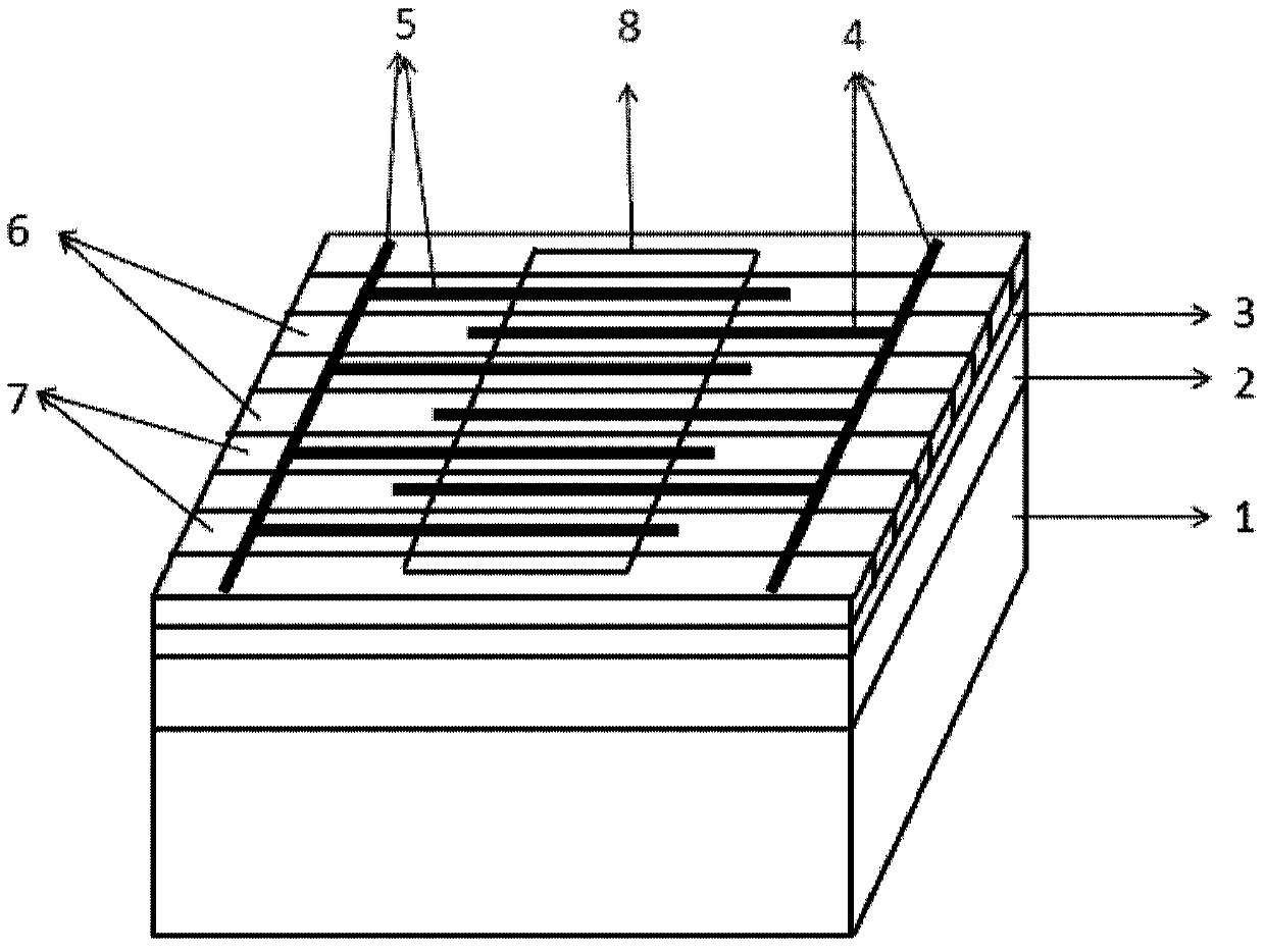
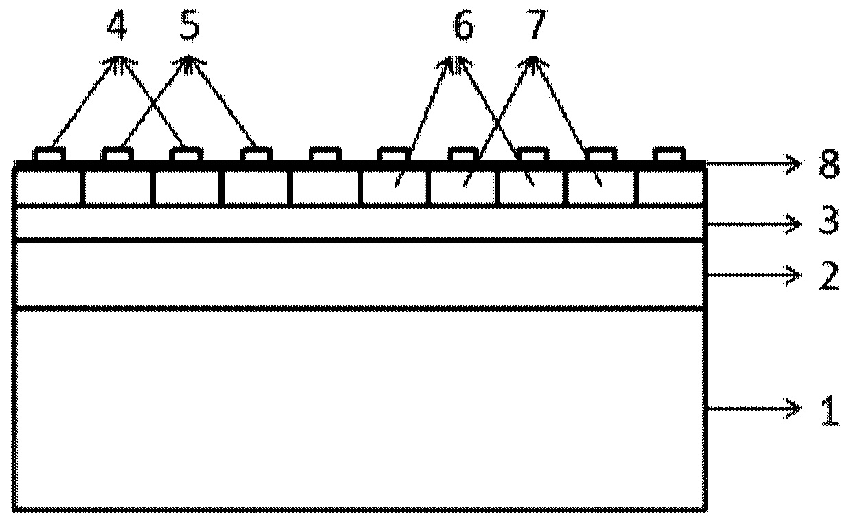
[0030] The present invention is a graphene photodetector designed based on the SOI substrate material. For different buried oxide layer thicknesses and top layer silicon thicknesses, the corresponding optimal design is also different to achieve functional requirements. Therefore, for convenience of description, the substrate of the present invention The material defaults to specific implementation parameters, that is, the thickness of the buried oxide layer is 3 μm, and the thickness of the top silicon layer is 220 nm.

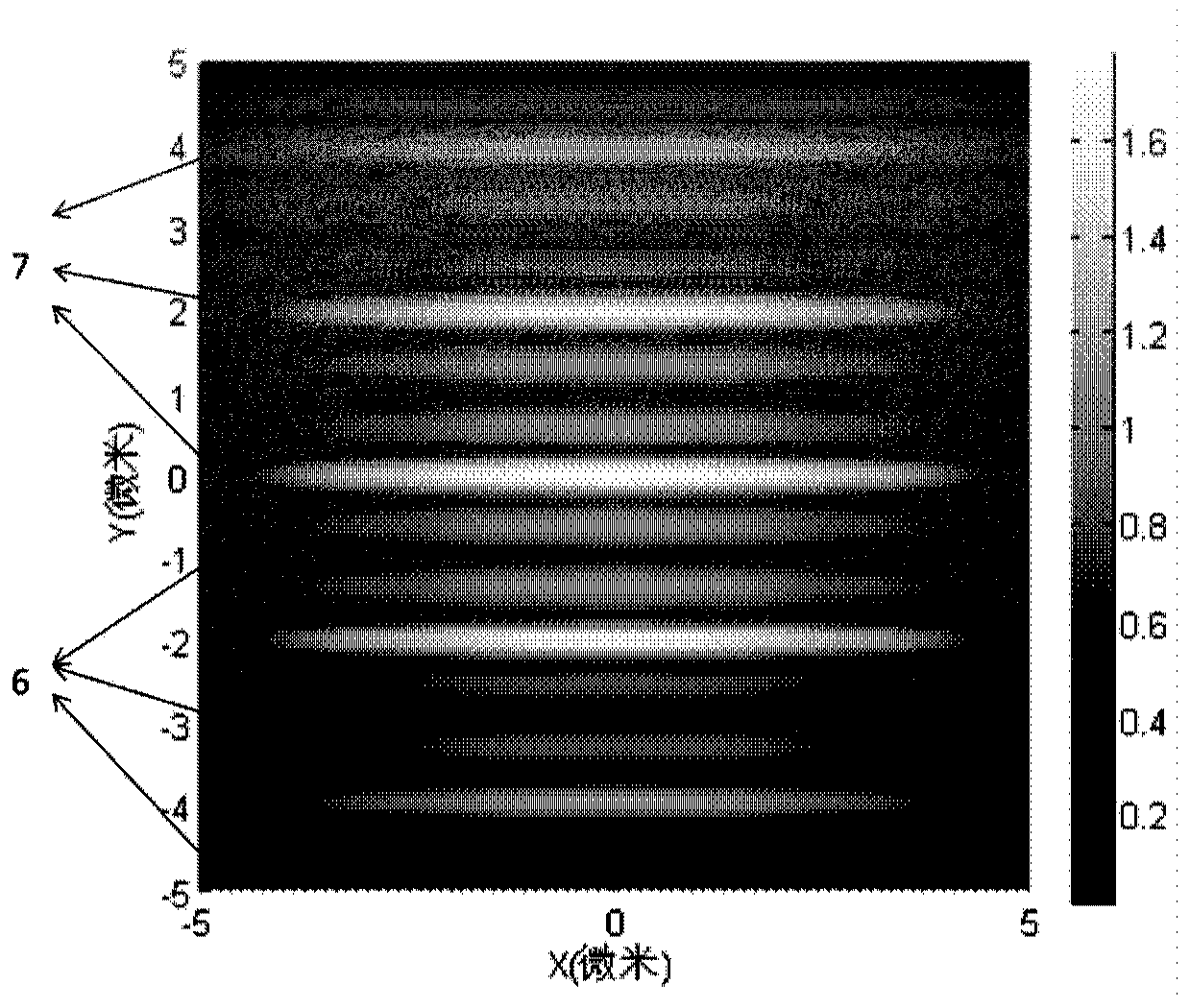
[0031] figure 1 It is a schematic diagram of the three-dimensional structure of the surface incident graphene photodetector based on the one-dimensional grating structure provided by the present invention...


PUM

PropertyMeasurementUnit
Thicknessaaaaaaaaaa
Thicknessaaaaaaaaaa
Thicknessaaaaaaaaaa

Abstract

The invention discloses a surface incidence graphene photoelectric detector based on one-dimensional optical grating. The surface incidence graphene photoelectric detector based on the one-dimensional optical grating comprises a silicon-on-insulator (SOI) substrate, the one-dimensional optical grating, a graphene layer (8), a first interdigital electrode (4) and a second interdigital electrode (5), wherein the SOI substrate sequentially includes silicon, a buried oxide layer and top layer silicon from bottom to top; the top layer silicon is etched to form the one-dimensional optical grating, and the one-dimensional optical grating is formed by alternate distribution of a plurality of silicon dioxide strips (6) and a plurality of silicon strips (7) and used for modulating the space distribution of an optical field which acts with the graphene layer; the graphene layer (8) is formed on the one-dimensional optical grating and serves as an active layer to act with the surrounding optical field to generate an electron hole pair; the first interdigital electrode (4) and the second interdigital electrode (5) are formed on the graphene layer (8), the first interdigital electrode (4) and the second interdigital electrode (5) are both in contact with graphene so as to form a built-in electric field on a contact surface, and the built-in electric field is used for effectively collecting photon-generated carriers to form light current. By means of the surface incidence graphene photoelectric detector based on the one-dimensional optical grating, the optical field of incident light around the graphene is modulated through a grating structure, and thereby, high response degree and high bandwidth of infrared detection can be achieved.

Description

technical field [0001] The invention relates to a surface incident graphene photodetector, in particular to a surface incident graphene photodetector based on a one-dimensional grating. Background technique [0002] Graphene was discovered in 2004. Just 6 years later, the two scientists who discovered it won the Nobel Prize in Physics. It can be seen that graphene is of great significance to scientific research and industrial production. Scientists soon discovered that graphene has many good properties that other materials do not have, and it also has excellent electrical, optical, and mechanical properties. In 2010, IBM successfully developed a graphene transistor with a cut-off frequency of 100 GHz on a silicon carbide substrate. Just one year later, graphene successfully realized integrated circuits. Graphene has unique optical and electrical properties due to its unique energy band structure. It has saturable absorption characteristics, and successfully realized a mode...

Claims


Application Information

Patent Timeline
IPC IPC(8): H01L31/0232H01L31/0224H01L31/101
CPCH01L31/02325H01L31/028H01L31/101
Inventor 黄北举程传同张赞张赞允陈弘达
Owner INST OF SEMICONDUCTORS - CHINESE ACAD OF SCI
Why Eureka
Try Eureka