Broadband flat plate array antenna
An array antenna, flat panel technology, applied to antennas, antenna arrays, resonant antennas, etc., can solve the problems of decreased gain bandwidth, unfavorable miniaturization, negative growth, etc., and achieve the effect of increasing gain, being conducive to miniaturization, and broadening bandwidth
- Summary
- Abstract
- Description
- Claims
- Application Information
AI Technical Summary
Problems solved by technology
Method used
Image
Examples
Embodiment 1
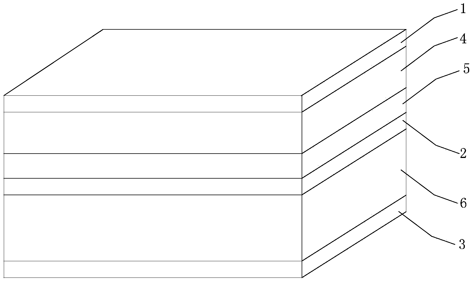
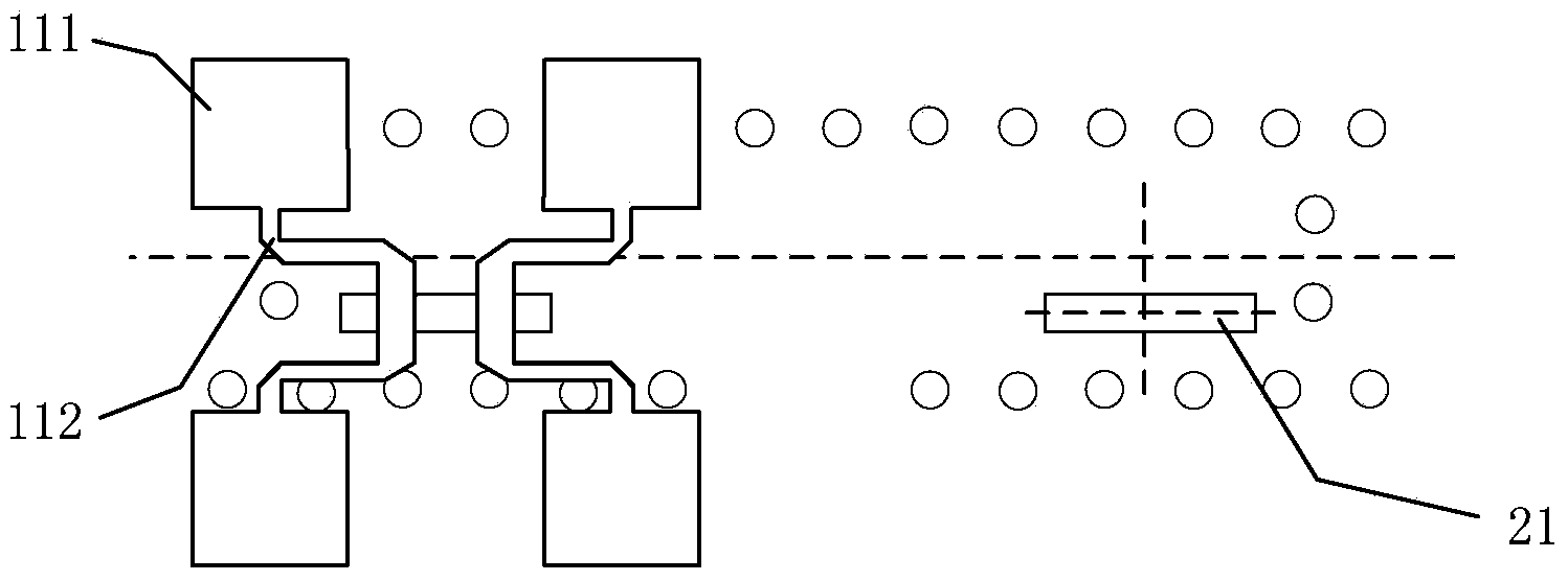
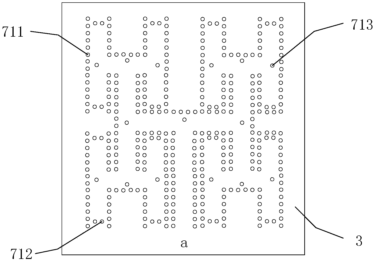
[0032]In this embodiment, the array of the broadband panel array antenna is a 4×4 array, and its center frequency is 61.5 GHz, and an electromagnetic full-wave simulation is performed on it in HFSS. The broadband panel array antenna includes a first metal copper-clad layer 1, a first dielectric layer 4, a second metal copper-clad layer 2, a second dielectric layer 6, an adhesive layer 5, a third Metal copper-clad layer 3, etched on the first metal copper-clad layer 1 are multiple groups of microstrip sub-arrays 11, and each group of microstrip sub-arrays 11 is composed of two microstrip patch units 111 and two microstrip patch units connected to each other. The microstrip feeder 112 of the chip unit 111; the second dielectric layer 6 is provided with a "I"-shaped substrate integrated waveguide feeding network, and the substrate integrated waveguide feeding network includes a plurality of substrate integrated waveguide units and power The sub-tuning hole 713, the substrate inte...
Embodiment 2
[0034] In this embodiment, the array of the broadband panel array antenna is a 32×32 array, and its center frequency is 61.5 GHz, and an electromagnetic full-wave simulation is performed on it in HFSS. The broadband panel array antenna includes a first metal copper-clad layer 1, a first dielectric layer 4, a second metal copper-clad layer 2, a second dielectric layer 6, an adhesive layer 5, a third Metal copper-clad layer 3, etched on the first metal copper-clad layer 1 are multiple groups of microstrip sub-arrays 11, and each group of microstrip sub-arrays 11 is composed of two microstrip patch units 111 and two microstrip patch units connected to each other. The microstrip feeder 112 of the chip unit 111; the second dielectric layer 6 is provided with a "I"-shaped substrate integrated waveguide feeding network, and the substrate integrated waveguide feeding network includes a plurality of substrate integrated waveguide units and power The sub-tuning hole 713, the substrate i...
PUM
 Abstract
Description
Claims
Application Information


