

High linearity optimization method for transconductance amplifier
A technology of transconductance amplifier and optimization method, which is applied in the design of the Internet of Things and related fields, can solve problems such as adding asymmetric source-level coupling pairs, affecting other units of the system or even system performance, sacrificing the difficulty of circuit design, etc., to achieve small linear distortion Effect
- Summary
- Abstract
- Description
- Claims
- Application Information
AI Technical Summary
Problems solved by technology
Method used
Image

Examples
Embodiment Construction
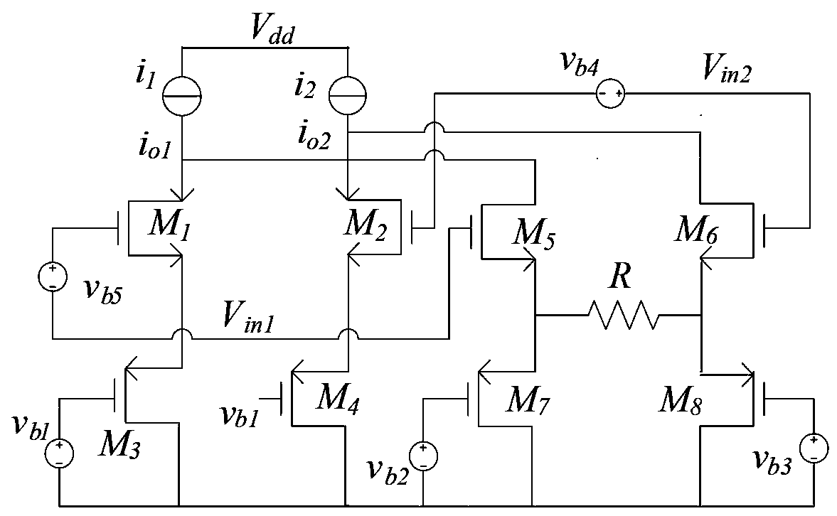
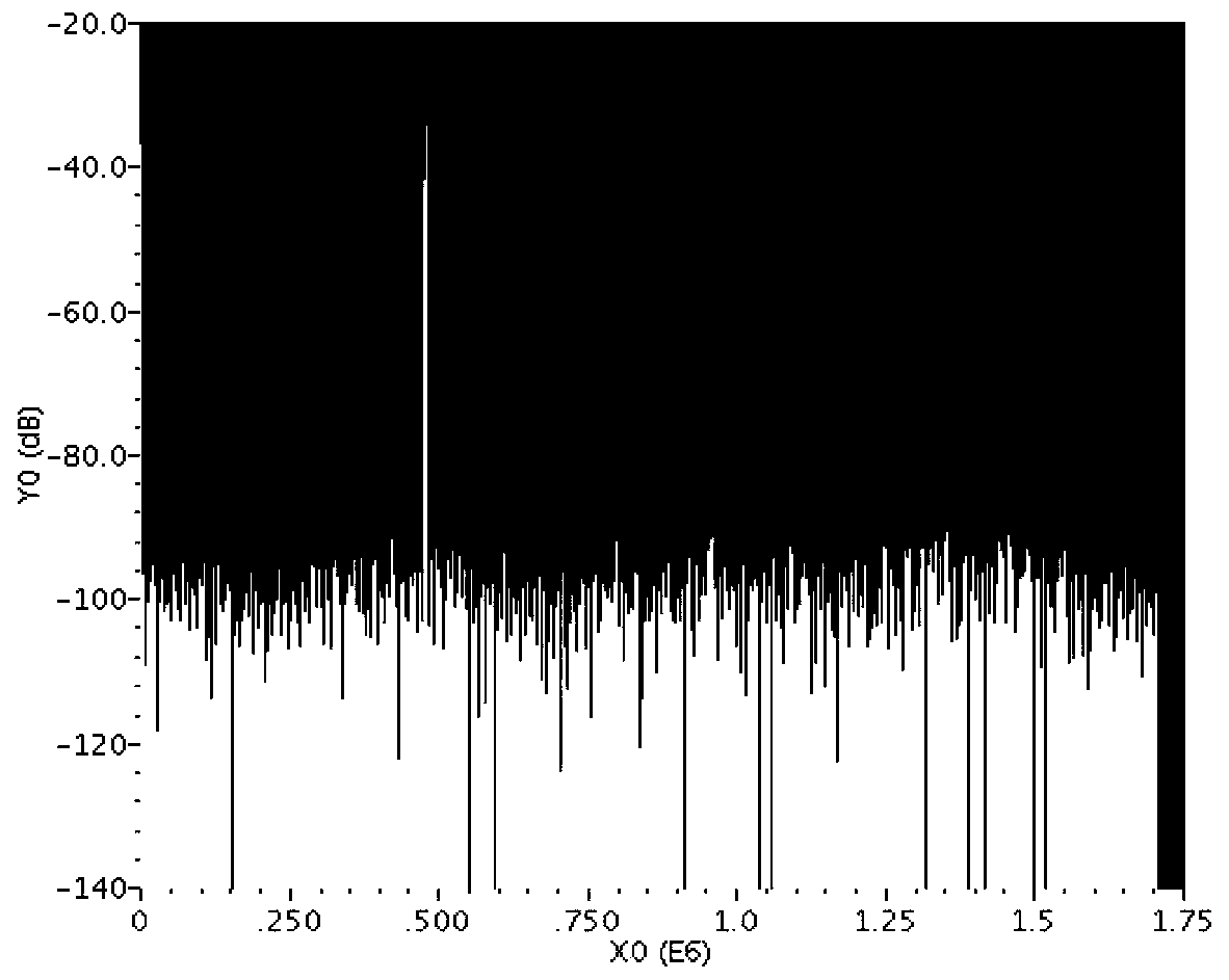
[0026] Such as figure 1 As shown, the circuit schematic diagram of the transconductance amplifier of Embodiment 1 of the present invention; figure 2 yes figure 1 Schematic diagram of the SFDR simulation results of the illustrated embodiment. In order to investigate the proposed linearity optimization method, this paper applies this method to the transconductor circuit of the first embodiment. The transconductors in this embodiment all adopt CMOS differential pairs, and the transconductance value of the transconductors is changed by adjusting the gate voltage. The sources of M5 and M6 are connected to resistance R, and the resistance R is constant at 1K ohms, and the deviation between Vb2 and Vb3 does not exceed 0.5V. The input signals Vin1 and Vin2 satisfy f(t - )=4f(t + ) / 3+1 condition.
[0027] M5 and M6 work at a lower common-mode voltage, which can effectively reduce linear distortion. At the same time, considering that the gate input of M5 and M6 should satisfy f(t...
PUM
 Abstract
Description
Claims
Application Information