
Anisotropy zero refractive index device with controllable switch

A zero-refractive-index, anisotropic technology, applied in the field of new artificial electromagnetic devices, can solve problems such as inability to change the working state and poor device flexibility, and achieve the effects of convenient adjustment, convenient processing, and light weight

Active Publication Date: 2014-06-04
SOUTHEAST UNIV
View PDF3 Cites 7 Cited by
  • Summary
  • Abstract
  • Description
  • Claims
  • Application Information

AI Technical Summary

Problems solved by technology

However, this zero-refractive-index device is less flexible, and its working state cannot be changed after the device is processed.

Method used


Image

  • Anisotropy zero refractive index device with controllable switch
  • Anisotropy zero refractive index device with controllable switch
  • Anisotropy zero refractive index device with controllable switch

Examples


Embodiment Construction

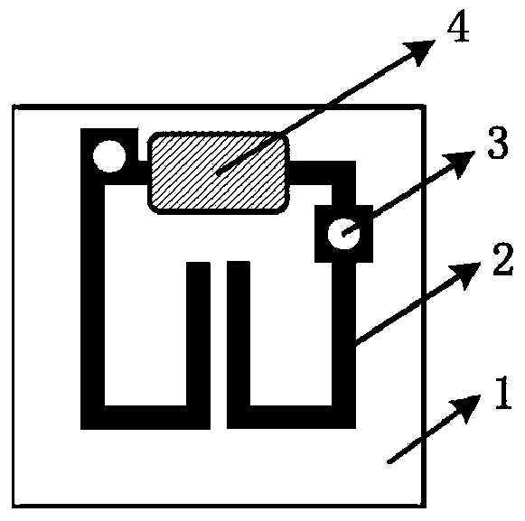
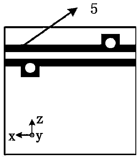
[0021] The switch-controllable zero refractive index device proposed by the present invention is composed of resonant units on the sub-wavelength scale arranged along a certain rule. The technical solution adopted by a single resonant unit is as follows: an open resonant ring unit structure 2 with an open upper end is processed on the upper surface of the dielectric substrate 1, and a PIN diode 4 is used to weld the upper end opening of the open resonant ring unit 2. Two metal strips 5 are processed on the lower surface of the dielectric substrate 1 to serve as DC feeders. Two metallized through holes 3 are made inside the dielectric substrate 1 to connect the DC feed line 5 and the positive and negative electrodes of the PIN diode 4 for applying a voltage bias to the PIN diode 4. Resonant unit model such as figure 1 As shown, figure 1 It is a front view of the resonant unit, the upper opening of the split resonant ring unit 2 is connected by a PIN diode 4; figure 2 For the ba...


PUM


Abstract

The invention provides an anisotropy zero refractive index device with a controllable switch. The device is formed by regularly arranging opening resonance ring units of a plurality of loading PIN diodes on the dimension of the sub-wavelength. Each single resonance unit comprises an opening resonance ring structure processed on the upper surface of a dielectric substrate, and the PIN diode welded between openings of the upper ends of the opening resonance ring units. Two metal straps are processed on the lower surface of the dielectric substrate and serve as direct-current feed wires. Two through metallization holes are formed in the dielectric substrate and used for connecting the direct-current feed wires and an anode and a cathode of each PIN diode. The anode and the cathode of each PIN diode are connected with the direct-current feed wires of the back of the dielectric substrate through one through metallization hole. All the direct-current feed wires are combined to form a feed network. The feed network of the lower surface of the dielectric substrate is divided into the positive portion and the negative portion, the positive portion and the negative portion are connected with the anodes and the cathodes of all the PIN diodes of each row respectively, and bias voltage is applied on all the PIN diodes on the upper surface of the dielectric substrate so as to change the working conditions of the PIN diodes.

Description

Technical field [0001] The invention relates to a switch-controllable zero-refractive index device used in microwave frequency bands, and belongs to the field of new artificial electromagnetic devices. Background technique [0002] The new type of artificial electromagnetic material (Metamaterials) in the present invention is an emerging research field in electromagnetics, and its basis is the theory of equivalent media, which is composed of a series of artificially designed units arranged in a certain rule on the sub-wavelength scale. By carefully designing the unit structure and size, the required equivalent dielectric constant and permeability can be obtained. After more than ten years of development, new artificial electromagnetic materials have been developed by leaps and bounds, and are widely used in stealth and antenna engineering. The anisotropic zero-refractive index device based on the new artificial electromagnetic material uses the equivalent electromagnetic paramet...

Claims


Application Information

Patent Timeline
Patent Type & Authority Applications(China)
IPC IPC(8): H01Q3/44H01Q23/00
Inventor 程强项楠赵捷陈洁崔铁军
Owner SOUTHEAST UNIV
Learn More