Manufacturing method for novel shadow mask for producing OLED display panel

A manufacturing method and display panel technology, applied in the direction of ion implantation plating, metal material coating process, coating, etc., can solve the problems of difficult control of etching precision, high etching rejection rate, and difficult chemical etching, etc. , to achieve the effects of shortening the etching cycle, simplifying the manufacturing process, and facilitating etching

Active Publication Date: 2014-06-18
ZHONGSHAN AISCENT TECH
View PDF4 Cites 15 Cited by
  • Summary
  • Abstract
  • Description
  • Claims
  • Application Information

AI Technical Summary

Problems solved by technology

But it is quite difficult to chemically etch the Invar shadow mask
One is that the etching thickness is too large, it is difficult to control the etching precision during the etching process, and the etching time is very long, usually it takes several days to etch; the other is that when etching, it must be coated on the etched surface However, during the etching process, the protective layer

Method used


Image

  • Manufacturing method for novel shadow mask for producing OLED display panel
  • Manufacturing method for novel shadow mask for producing OLED display panel
  • Manufacturing method for novel shadow mask for producing OLED display panel

Examples


Embodiment Construction

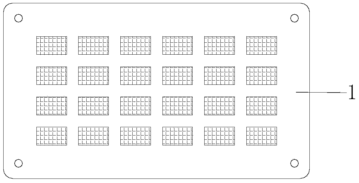
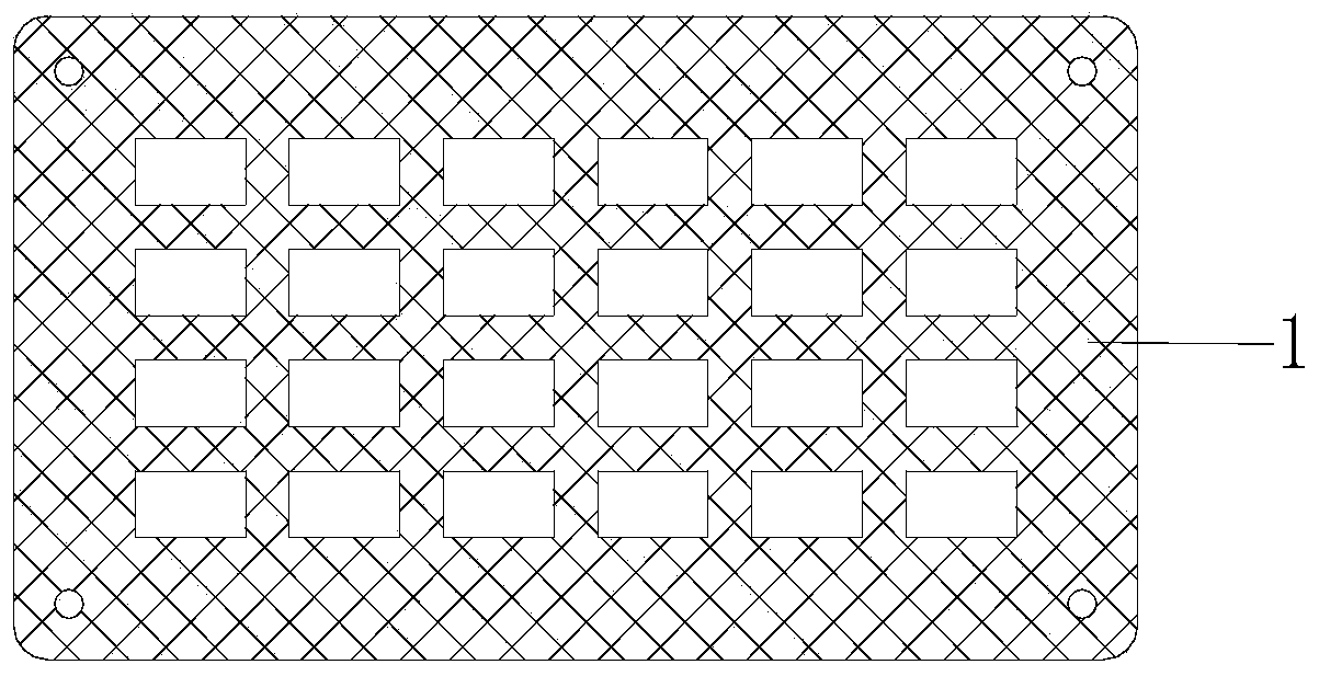
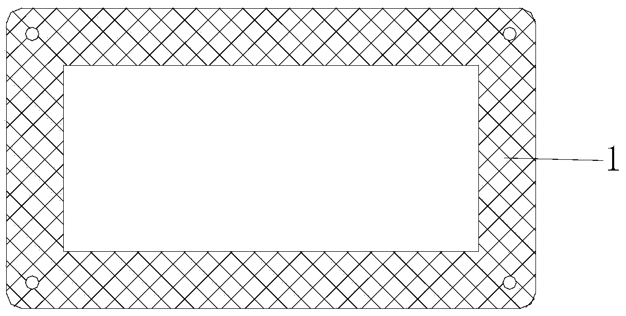
[0047] A method for making a novel shadow mask for OLED display panel production, the structure of the shadow mask 1 is as follows: figure 1 , figure 2 , image 3 As shown, in this embodiment, only the creation of a fine graphics area is taken as an example for illustration.

[0048] 1. Preparation of substrate or frame

[0049] Made of stainless steel or Invar (Invar) such as Figure 4 , Figure 5 Substrate or frame workpiece with single or multiple through holes2 as shown. According to the size and complexity of the fine mask plate, there may be one or more through holes. The size of the through hole is 0.5-3mm longer than each side of the mask pattern actually required, and the center of the through hole coincides with the center of the mask pattern. The reason why the size of the through hole is 0.5-3mm longer than the sides of the actual required mask pattern is: one is that the present invention adopts the method of inlaying fillers, in order to ensure the one-to-...


PUM


Abstract

The invention discloses a manufacturing method for a novel shadow mask for producing an OLED display panel. The manufacturing method comprises the steps of preparing a substrate or a framework workpiece, processing an alignment marker, embedding a filler, coating a photosensitive layer, performing exposure, development and plasma activation treatment, protecting a non-electric depositional surface, electrically depositing a fine mask, removing the photosensitive layer, removing the filler and the like. The filler is very convenient to remove and etch; in an etching process, a protection layer does not need to be added, and the filler etching work can be finished within 2-3 hours, so that the etching period is greatly shortened, and the production cost of a product is lowered. According to the shadow mask manufactured by the method disclosed by the invention, the fine mask and the substrate or the framework are tightly combined to form an integrated structure; on one hand, the process for welding the fine mask on a border is canceled, and the manufacturing process is simplified; on the other hand, an inner separation frame on the substrate or the framework can achieve a certain supporting and protecting effect in a corresponding operation process for cleaning and OLED evaporation, so that drop-down of the fine mask is alleviated, and the service life of the shadow mask is greatly prolonged.

Description

technical field [0001] The invention relates to a method for manufacturing a shadow mask for OLED display panel production, and belongs to the technical field of semiconductor manufacturing. Background technique [0002] The production of high-pixel-density OLED (organic light-emitting diode, also known as organic laser display, which has self-luminous characteristics) display panels requires the use of fine metal masks (Fine Metal Mask, FMM) with very thin thickness and small thermal expansion coefficient. The shadow mask (or mask) is used to evaporate the organic luminous body (three primary colors) in the pixel of the OLED panel. [0003] At present, the shadow mask for OLED is usually prepared by using Invar alloy (INVAR, also known as Invar) by chemical etching. First, apply photoresist or photosensitive dry film on the surface of Invar alloy, transfer the fine pattern of the mask plate to the photosensitive film by exposure, and finally make a shadow mask plate by dev...

Claims


Application Information

Patent Timeline
IPC IPC(8): C23C14/04
Inventor 李源韩建崴杜卫冲
Owner ZHONGSHAN AISCENT TECH
Why Eureka
Try Eureka