Reaction unit and method for atom layer film deposition

A thin film deposition and reaction device technology, which is applied in the direction of coating, metal material coating process, gaseous chemical plating, etc., can solve the problems of uneven distribution, slow deposition rate, weak power, etc., to reduce the temperature gradient, Effect of shortening heating time and improving uniformity

Active Publication Date: 2014-06-18
BEIJING NAURA MICROELECTRONICS EQUIP CO LTD
View PDF6 Cites 9 Cited by
  • Summary
  • Abstract
  • Description
  • Claims
  • Application Information

AI Technical Summary

Problems solved by technology

However, this device has the following defects: (1) the silicon wafer carrying unit can only carry one silicon wafer at a time, the silicon wafers for depositing thin films have low productivity and high equipment cost; (2) the gaseous reaction precursor is vertically sprayed on the center of the silicon wafer surface, and the Diffusion from the center of the silicon wafer to the surroundings leads to low utilization of gaseous reaction precursors; (3) gaseous reaction precursors and reaction by-products are likely to remain at the bottom of the silicon wafer carrying unit, which is difficult to empty, resulting in the formation of gas field vortex areas, gas field vortex areas The gaseous reaction precursors and reaction by-products in the interior are difficult to evacuate, and the residues adhere to the surface of the silicon wafer, resulting in a decrease in the quality of atomic layer film deposition
However, this device has the following defects: (1) increasing the number of silicon wafer carrying units increases the production capacity of silicon wafers, resulting in a complex structure of the reaction chamber, high processing and maintenance costs, and a limited increase in the number of silicon wafers; The remaining gaseous reaction precursors between the unit and the silicon wafer are difficult to empty, and the residue adheres to the surface of the silicon wafer, resulting in a decrease in the deposition quality of the atomic layer film; (3) the uneven distribution of the heating units in the reaction chamber makes the inner wall of the reaction chamber There is a temperature gradient on the surface, so that there is a temperature gradient on the surface of the silicon wafer, resulting in uneven thickness of the atomic layer film on the surface of the silicon wafer; (4) The path from the gaseous reaction precursor to the surface of the silicon wafer is L-shaped, which can only be reached after a right-angle turn Wafer surface, therefore, the kinetic energy of the gaseous reactive precursors to reach the wafer surface is not strong
[0006] To sum up, those skilled in the art need to develop a new reaction device for atomic layer film deposition to solve the problem of low productivity of silicon wafers and temperature gradients on the surface of silicon wafers in existing reaction devices. Problems such as uneven distribution on the surface of the sheet, slow deposition rate, and inability to evacuate gaseous reaction precursors

Method used


Image

  • Reaction unit and method for atom layer film deposition
  • Reaction unit and method for atom layer film deposition
  • Reaction unit and method for atom layer film deposition

Examples


Embodiment 1

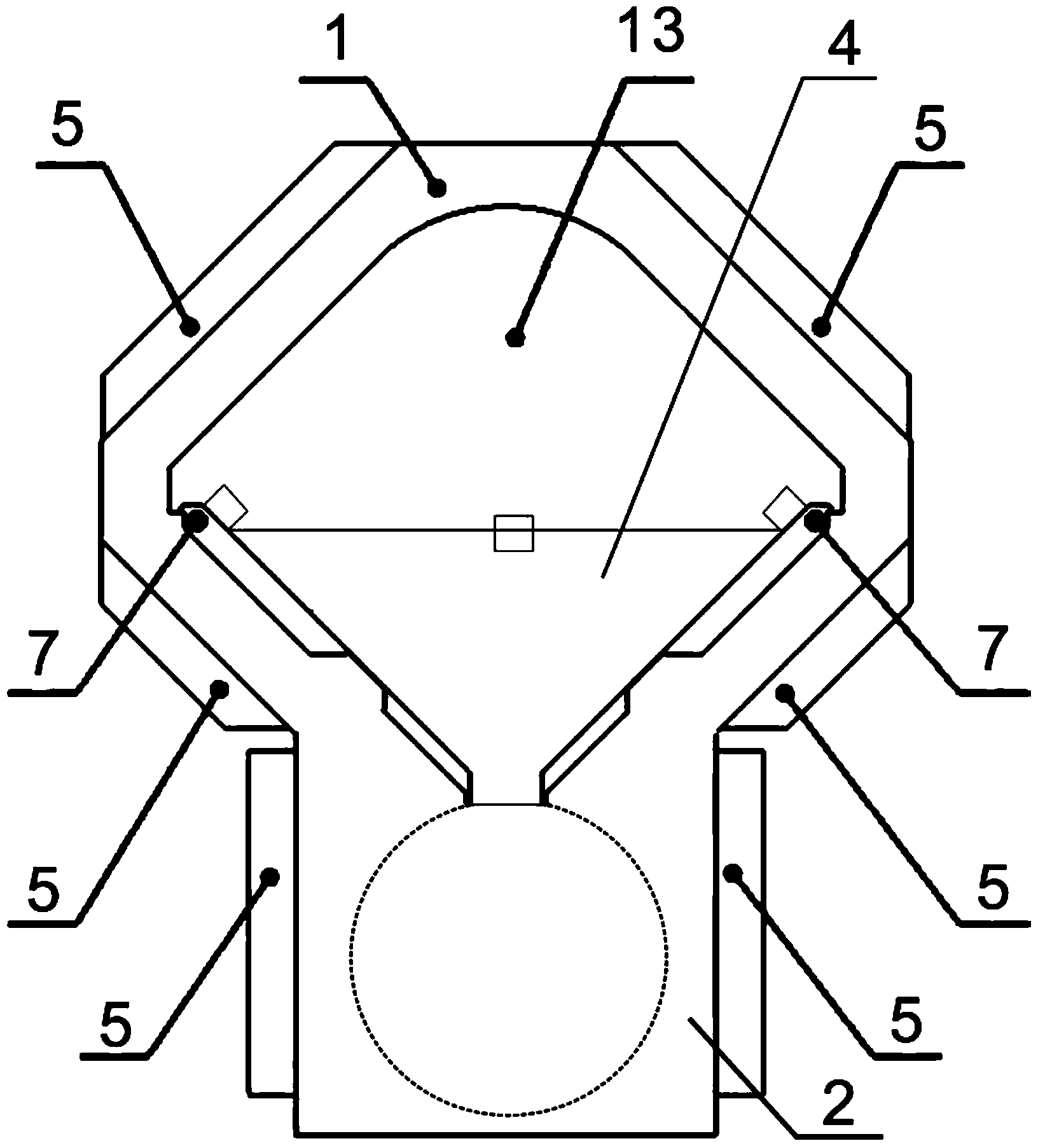
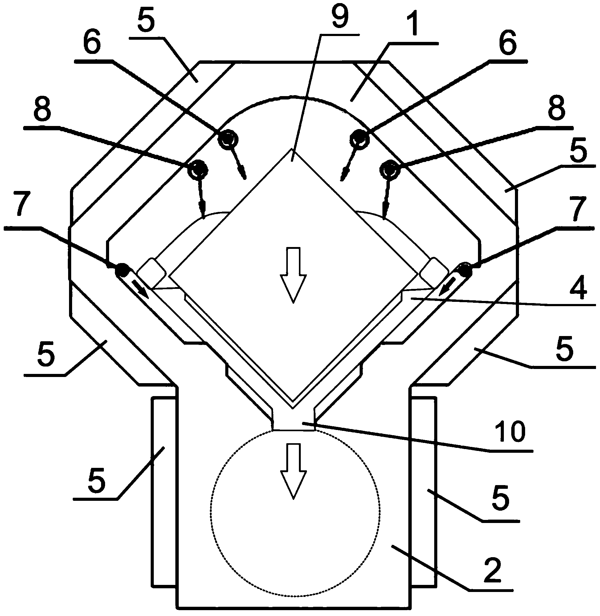
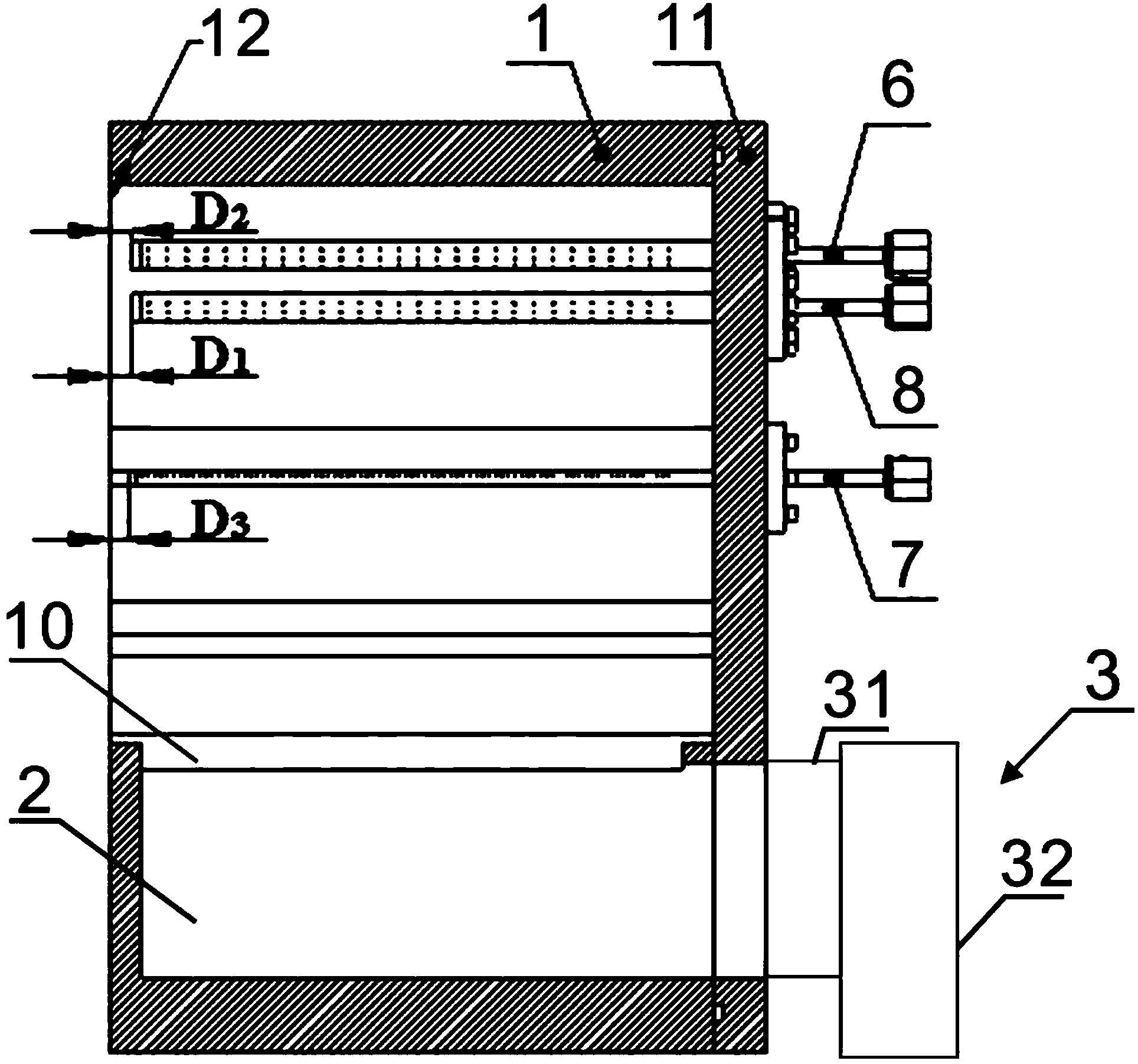
[0052] like Figure 1 to Figure 4 As shown, the present invention provides a reaction device for atomic layer thin film deposition, comprising: a reaction deposition chamber 1, a reaction evacuation chamber 2 and a vacuum system 3; The reaction evacuation chamber 2 is connected, and the reaction evacuation chamber 2 is connected to the vacuum system 3, and the vacuum system 3 is used to pump air to the reaction evacuation chamber, so that the reaction deposition chamber 1 is in the vacuum state; wherein, the reaction deposition chamber 1 includes a silicon wafer carrying unit 4, a heating unit 5, a precursor feeding unit 6, and a purge gas intake unit 7; the silicon wafer carrying unit 4 is provided with several silicon The wafer carrying position and the bottom of the silicon wafer carrying unit are provided with some ventilation holes, and the silicon wafer carrying unit 4 is provided with a shield cover 13 for sealing the reaction deposition chamber 1; the heating unit 5 is...

Embodiment 2

[0069] On the basis of implementing one, the difference from Example one is: the internal pressure of the reaction deposition chamber 1 is 3Torr, and the first gaseous reaction precursor is trimethylaluminum (TMA) and ozone (O 3 ), the second gaseous reaction precursor is ozone (O 3 ); the angle β1 between the direction of the air outlet of the precursor feeding unit 6 and the wall of the reaction deposition chamber 1 is 90°, and the distance D2 between the end of the heating gas inlet unit 8 and the front face 12 of the reaction chamber is 3mm. The reaction chamber in the present embodiment can complete the deposition of Al with a thickness of 20nm to 250 P-type silicon wafers 9 every 30 minutes. 2 o 3 Thin film, production capacity up to 500 pieces / hour.


PUM


Abstract

The invention provides a reaction unit and a method for atom layer film deposition, and belongs to the technical field of manufacturing, assembly and processing of solar cells. The reaction unit comprises a reaction deposition chamber, a reaction emptying chamber and a vacuum system connected in sequence, wherein a silicon wafer bearing unit, a heating unit, a precursor feeding unit and a blowing gas charging unit are arranged inside the reaction deposition chamber. According to the method disclosed by the invention, at least two gaseous precursors are fed into a reactor in a pulse alternation manner and chemically adsorbed on a depositing base body for reaction so as to form a deposited film. The reaction unit and the method disclosed by the invention have the advantages of effectively remedying the defects that in the existing reaction unit, the productivity is low, the gaseous reactant precursors are distributed on the surface of the silicon wafer unevenly, temperature gradient exists on the surface of the silicon wafer and the gaseous reactant precursors cannot be discharged completely and the like, greatly improving the productivity and the depositing speed of the silicon wafer of an atom layer film depositing device and effectively improving the deposition quality of the atom layer film.

Description

technical field [0001] The invention belongs to the technical field of solar cell manufacturing, assembly and processing, and in particular relates to a reaction device and method for atomic layer film deposition. Background technique [0002] As the solar cell process technology continues to advance, the requirements for the thickness uniformity and quality of the thin film process are increasing day by day. The traditional CVD deposition technology has been difficult to effectively control the film characteristics and meet the increasingly stringent technical requirements. Atomic Layer Deposition (ALD) was originally called Atomic Layer Epitaxy (ALE). It is called atomic layer chemical vapor deposition (Atomic Layer Chemical Vapor Deposition, ALCVD), which uses the gas-solid phase reaction between the reaction gas and the substrate to complete the process requirements. Because it can complete the process with high precision, it is regarded as One of the key links in the d...

Claims


Application Information

Patent Timeline
Patent Type & Authority Applications(China)
IPC IPC(8): C23C16/44
Inventor 潘龙刘东彭文芳常青
Owner BEIJING NAURA MICROELECTRONICS EQUIP CO LTD
Why Eureka
Try Eureka