Gettering method through implantation of carbon ions

A carbon ion implantation and ion implantation technology, which is applied in the field of gettering, can solve the problems of difficult removal of metal impurities, existence of white pixels, and poor imaging quality of CMOS sensors, and achieves the effects of high compatibility, reduced dark current, and improved imaging effects.

Inactive Publication Date: 2014-06-18
WUHAN XINXIN SEMICON MFG CO LTD
View PDF5 Cites 5 Cited by
  • Summary
  • Abstract
  • Description
  • Claims
  • Application Information

AI Technical Summary

Problems solved by technology

[0003] The technical problem to be solved by the present invention is to provide a method of using carbon ion implantation to get rid of impurities, which solves the problems in the prior art that metal impurities are difficult to remove, the imaging quality of CMOS sensors is poor, and there are white pixels.

Method used


Image

  • Gettering method through implantation of carbon ions
  • Gettering method through implantation of carbon ions
  • Gettering method through implantation of carbon ions

Examples


Embodiment Construction

[0016] The principles and features of the present invention are described below in conjunction with the accompanying drawings, and the examples given are only used to explain the present invention, and are not intended to limit the scope of the present invention.

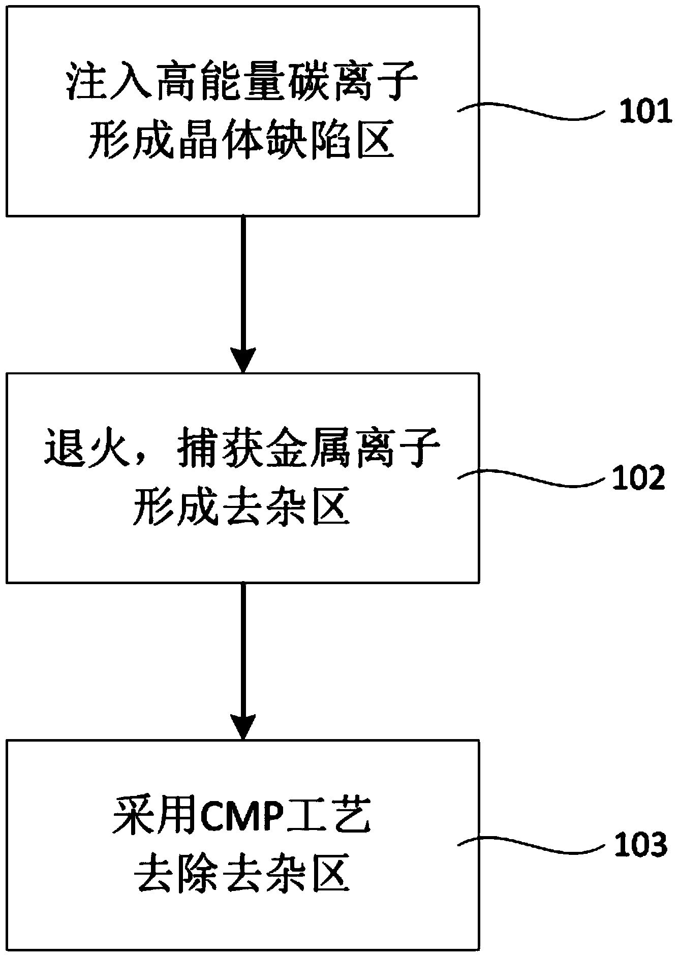
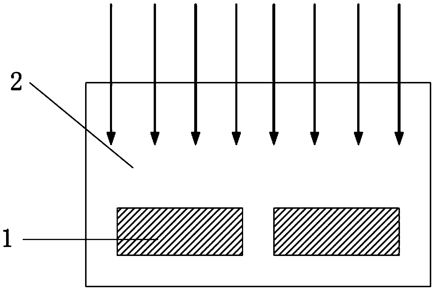
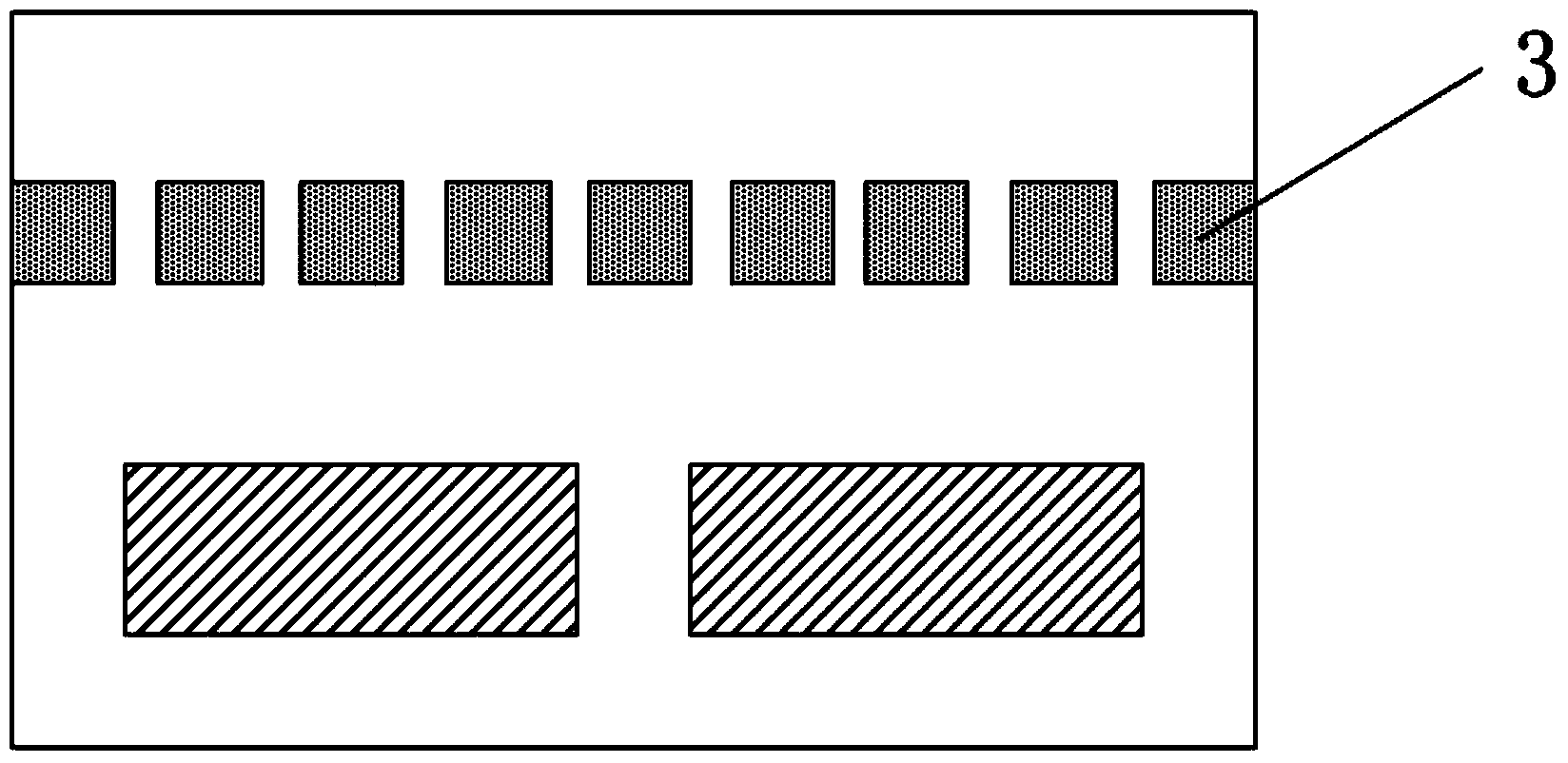
[0017] Such as figure 1 Shown is the flowchart of the carbon ion implantation gettering method of the present invention, Figure 2a-2c It is a structural diagram corresponding to the carbon ion implantation gettering method of the present invention. Method of the present invention comprises the following steps:

[0018] Step 101, before the emission junction of the photodiode 1 is formed, a certain energy and a certain dose of high-energy carbon ions are implanted through the exposed layer on the back of the silicon wafer 2 through an ion implantation process, and a crystal defect region 3 is formed in the implanted layer of the silicon wafer, Such as Figure 2a , 2b shown; preferably, the implantation energy of...


PUM

PropertyMeasurementUnit
Thicknessaaaaaaaaaa

Abstract

The invention relates to a gettering method through implantation of carbon ions. The method comprises the following steps that high-energy carbon ions are implanted on an exposed layer on the back face of a silicon wafer or a silicon dioxide layer on the back face of the silicon wafer by the adoption of the ion implantation process, and a crystal defect area is formed on the implantation layer of the silicon wafer; the annealing is carried out, the crystal defect area is converted to be a gettering area, and metal ions in the silicon wafer are captured to form an impurity removing area; the impurity removing area is removed according to the chemical and mechanical grinding method. The ion implantation gettering process and the manufacturing process of a photodiode are high in compatibility and can be easily added into the prior art, the carbon ion implantation has no side effect on the performance of a device, and the device is not polluted in the gettering process of the ion implantation; meanwhile, the ion implantation gettering process parameters are optimized and controlled, so that the metal ion gettering effect is good, the performance of the gettered photodiode is better remarkably, dark current and white pixels are reduced remarkably, and the imaging effect of a CMOS sensor is improved.

Description

technical field [0001] The invention relates to a gettering method, in particular to a gettering method utilizing carbon ion implantation. Background technique [0002] Photodiodes are semiconductor devices that convert light signals into electrical signals. Its core part is a PN junction, which has been widely used in the field of CMOS sensors. In the manufacturing process of photodiodes, metal contamination problems are inevitable due to hardware materials and manufacturing processes of the machine, and excessive metal concentration will affect the imaging quality of CMOS sensors, resulting in white pixels. The existing technology usually adopts the method of suppressing or removing metal sources to solve metal pollution, that is, to strictly control the manufacturing environment and manufacturing process, and try to maintain an "ultra-clean" working state. This method not only has limited effects, but also greatly increases production costs. , unable to meet the higher ...

Claims


Application Information

Patent Timeline
IPC IPC(8): H01L31/18H01L21/265
CPCH01L21/322H01L21/26506H01L31/1804
Inventor 洪齐元黄海
Owner WUHAN XINXIN SEMICON MFG CO LTD
Why Eureka
Try Eureka