Electroluminescent device

A technology of electroluminescent devices and light-emitting layers, which is applied in the direction of electric solid-state devices, electrical components, semiconductor devices, etc., and can solve problems such as low lifespan and slow switching speed

Active Publication Date: 2014-06-18
ZHEJIANG BRILLIANT OPTOELECTRONIC TECH CO LTD
View PDF58 Cites 22 Cited by
  • Summary
  • Abstract
  • Description
  • Claims
  • Application Information

AI Technical Summary

Problems solved by technology

However, mobile ions also cause slow switching speed and low lifetime of the device.

Method used


Image

  • Electroluminescent device
  • Electroluminescent device
  • Electroluminescent device

Examples


Embodiment Construction

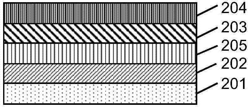
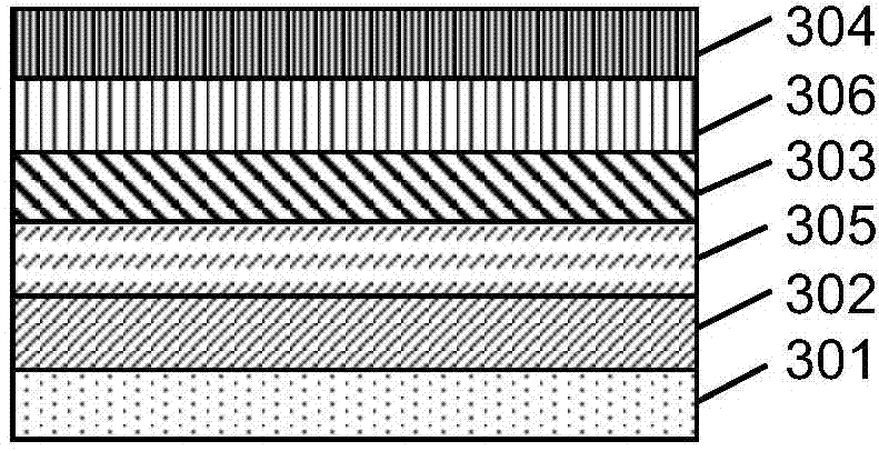
[0165] 1. Preparation of Cathode / FTL

[0166] The present invention uses 50nm ITO as the cathode. The ITO conductive glass substrate is first cleaned with various solvents (chloroform→acetone→isopropanol), and then treated with ultraviolet ozone plasma. Next, in a monolithic reactor, about 8 nm of TiN (TiCl 4 / NH 3) onto ITO by chemical vapor deposition. Hafnium oxide zirconia solid solution (Hf 0.5 Zr 0.5 o 2 ) were deposited on TiN by thermal atomic layer deposition (ALD). The ALD process was based on commercially available (Aldrich) organometallic precursors tetrakis-(ethylmethylamino)-(hafnium / zirconium) (TEMAH and TEMAZ) with ozone. The content of zirconia and hafnium oxide in the solid solution can be determined by changing the period ratio of the precursors. The thickness of the film is set to about 9nm by controlling the super period number of ALD. Then, the hafnium oxide zirconia solid solution film was heat-treated at 500°C for 5 minutes. Hf so prepared 0.5...


PUM


Abstract

The invention relates to a new electroluminescent device, in particular to a light emitting diode (LED) and an inorganic semiconductor lighting quantum dot or organic lighting material-based LED. The device comprises a ferroelectric thin layer (FTL) with ferroelectric performance or comprising a ferroelectric material. The invention also relates to the device structure and a production method of the electroluminescent device. The invention also relates to the application of the electroluminescent device in the lighting and display technologies and other occasions.

Description

Technical field: [0001] The present invention relates to a novel electroluminescence device, especially a light-emitting diode, especially a light-emitting diode based on quantum dots or organic light-emitting materials, its device structure, its production method and its application in lighting and display technology and other occasions in the application. Background technique: [0002] Thin-film electroluminescent devices, especially organic light-emitting diodes (OLEDs) (see TANG et al. Appl. Phys. Lett. 1987, 51, p913), and quantum dot light-emitting diodes (QDLEDs) (see Allvisatos et al. Due to its self-luminescence, high brightness, rich color tunability through chemical synthesis, and flexibility, it has become the most promising next-generation display and lighting technology. In particular, they may form films from solutions by printing methods, such as inkjet printing (InkJet Printing), screen printing (Screen Printing) and other technologies, which can greatly re...

Claims


Application Information

Patent Timeline
Patent Type & Authority Applications(China)
IPC IPC(8): H01L51/50H01L51/54
CPCH10K59/122H10K30/865H10K50/17H10K50/171
Inventor 潘才法
Owner ZHEJIANG BRILLIANT OPTOELECTRONIC TECH CO LTD
Why Eureka
Try Eureka