

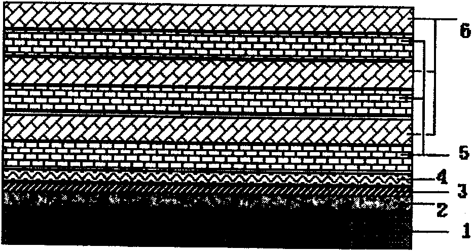
Strontium bismuth tantalate-strontium barium titanate heterogeneous dielectric material and synthesizing method and application thereof
A technology of strontium bismuth tantalate and strontium barium titanate, which is applied in the field of microelectronics, can solve the problems of difficult MOS tube leakage current indicators, affecting the performance of MOS tubes and chips, and easy fatigue, and achieves low power consumption, low operating temperature, good performance
- Summary
- Abstract
- Description
- Claims
- Application Information
AI Technical Summary
Problems solved by technology
Method used
Image

Examples
Embodiment 1
[0025] Except for the following differences, the rest are the same as the specific operation steps of the synthesis method of strontium bismuth tantalate-strontium barium titanate heterogeneous dielectric material in the summary of the invention.
[0026] In the first step, the thickness of the Ti layer is 5 nm, the thickness of the Pt electrode is 50 nm, and the deposition rate of the Ti layer or Pt electrode is 1 / sec; in the second step, pre-fire at 900°C, sinter at 1200°C, x=0.1; in the third step, the laser model is Lambda Physik LPX220icc, the pulse frequency is 5Hz, and it passes through a lens with a focal length of 45cm Focus the incident laser light on the strontium bismuth tantalate or strontium barium titanate target respectively in time, the distance between the substrate electrode and the target is 2cm, and the diameter between the substrate electrode and the target near the substrate electrode is 3cm The glow discharge ring, the substrate electrode is at 25 ℃, a...
Embodiment 2
[0028] Except for the following differences, the rest are the same as the synthesis method of the strontium bismuth tantalate-strontium barium titanate heterogeneous dielectric material in the summary of the invention.
[0029] In the first step, the thickness of the Ti layer is 15 nm, the thickness of the Pt electrode is 75 nm, and the deposition rate of the Ti layer or Pt electrode is 2 / sec; in the second step, pre-fire at 950°C, sinter at 1300°C, x=0.5; in the third step, the laser model is Lambda Physik LPX220icc, the pulse frequency is 10Hz, and passes through a lens with a focal length of 45cm Focus the incident laser light on the strontium bismuth tantalate or strontium barium titanate target respectively in time, the distance between the substrate electrode and the target is 10cm, and the diameter between the substrate electrode and the target near the substrate electrode is 9cm The glow discharge ring, the substrate electrode is heated to 160°C, a voltage of 400V is...
Embodiment 3
[0031] Except for the following differences, the rest are the same as the synthesis method of the strontium bismuth tantalate-strontium barium titanate heterogeneous dielectric material in the summary of the invention.
[0032] In the first step, the thickness of the Ti layer is 25 nm, the thickness of the Pt electrode is 100 nm, and the deposition rate of the Ti layer or Pt electrode is 3 / sec; in the second step, pre-fire at 1000°C, sinter at 1400°C, x=0.9; in the third step, the model of the laser is Lambda Physik LPX220icc, the pulse frequency is 15Hz, and it passes through a lens with a focal length of 45cm Focus the incident laser light on the strontium bismuth tantalate or strontium barium titanate target respectively in time, the distance between the substrate electrode and the target is 15cm, and the distance between the substrate electrode and the target near the substrate electrode is 15cm The glow discharge ring, the substrate electrode is heated to 300°C, a volta...
PUM
| Property | Measurement | Unit |
|---|---|---|
| thickness | aaaaa | aaaaa |
| thickness | aaaaa | aaaaa |
| thickness | aaaaa | aaaaa |
Abstract
Description
Claims
Application Information