Optical component for passive coupling of chip array and parallel optical fiber and its assembly method

A chip array and optical component technology, applied in the coupling of optical waveguides, etc., can solve the problems of complex process and long time consumption, and achieve the effect of simple production process, short time consumption and easy realization

Inactive Publication Date: 2016-05-11
昆山柯斯美光电有限公司
View PDF7 Cites 0 Cited by
  • Summary
  • Abstract
  • Description
  • Claims
  • Application Information

AI Technical Summary

Problems solved by technology

[0005] In order to solve the above technical problems, the present invention proposes an optical component for passive coupling of chip arrays and parallel optical fibers and an assembly method thereof. The optical component has a simple structure and low manufacturing cost, and high-precision and high-quality fast coupling can be realized through the optical component. It solves the problems of complex process and long time-consuming existing in the existing parallel optical fiber active coupling alignment method, and has high alignment accuracy, high coupling efficiency, and is easy to implement. It is suitable for various products using parallel optical fiber technology

Method used


Image

  • Optical component for passive coupling of chip array and parallel optical fiber and its assembly method
  • Optical component for passive coupling of chip array and parallel optical fiber and its assembly method
  • Optical component for passive coupling of chip array and parallel optical fiber and its assembly method

Examples


Embodiment Construction

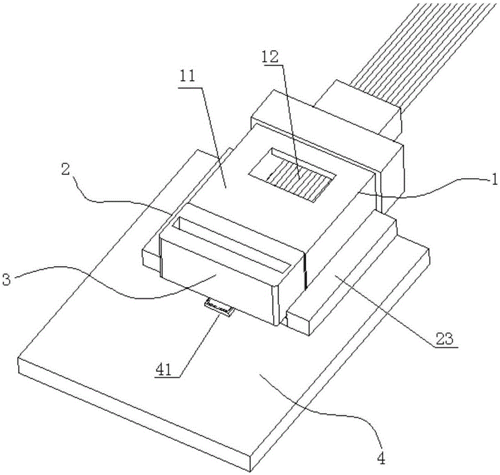
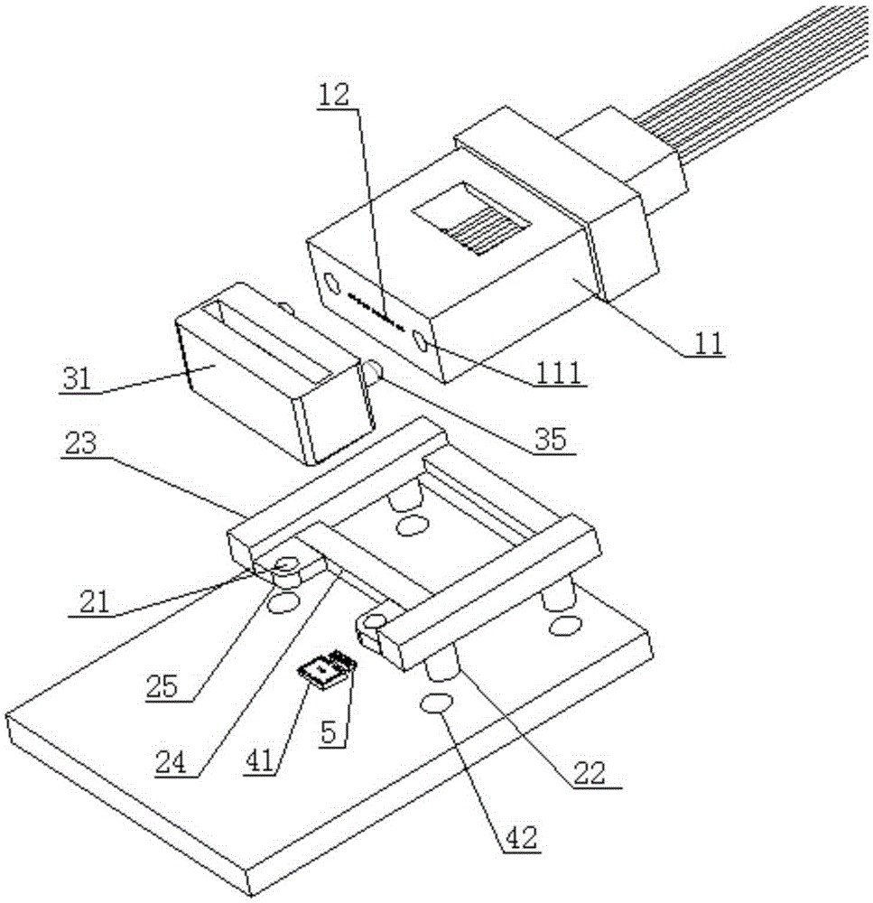
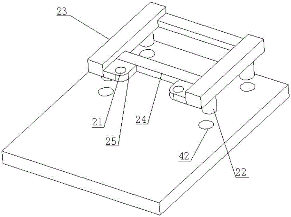
[0043] Such as figure 1 with figure 2 As shown, an optical assembly passively coupled between a chip array and parallel optical fibers includes an optical fiber array assembly 1, a coupling alignment positioning block 2, a lens array 3, a chip carrier 4, and at least one with a plurality of photoelectric conversion regions 51 (such as the light-emitting area of ​​the VCSEL chip array or / and the photosensitive area of ​​the PD chip array) the photoelectric chip array 5 (such as the VCSEL chip array or / and the PD chip array); Multiple parallel optical fibers 12 arranged in the fixed seat; the lens array includes a lens body 31, a second lens array surface 32 embedded in the lens body in the vertical direction corresponding to a plurality of photoelectric conversion regions, The first lens array surface 33 corresponding to the multi-channel parallel optical fiber embedded in the lens body in the horizontal direction and the first lens array surface 33 embedded in the lens body...


PUM


Abstract

The invention discloses a chip array and parallel optical fiber passively-coupled optical assembly which comprises an optical fiber array assembly, a coupling alignment positioning block, a lens array, a chip carrier and a photoelectric chip array. The optical fiber array assembly comprises a fixing base and a plurality of parallel optical fibers. The lens array comprises a lens body, a second lens array face, a first lens array face and a reflection face. The photoelectric chip array is pasted to the chip carrier, the coupling alignment positioning block is positioned on the chip carrier, the lens array is positioned on one side of the optical fiber array assembly, the lens array and the optical fiber array assembly are jointly positioned on the coupling alignment positioning block, the lens array and the coupling alignment positioning block are positioned in the mode that guiding columns are fixedly inserted in guiding holes, and the lens array and the fixing base are positioned in the mode that guiding columns are fixedly inserted in guiding holes. The chip array and parallel optical fiber passively-coupled optical assembly is simple in structure and low in manufacturing cost, high-accuracy and high-quality rapid coupling can be achieved through the chip array and parallel optical fiber passively-coupled optical assembly, and the chip array and parallel optical fiber passively-coupled optical assembly is suitable for various products with the parallel optical fiber technology.

Description

technical field [0001] The invention relates to the technical field of active optical cables, in particular to an optical component passively coupled with a chip array and parallel optical fibers and an assembly method thereof. Background technique [0002] In order to meet people's increasing demand for communication bandwidth, increasing transmission capacity and reducing power consumption are the top priorities in the field of optical fiber communication, and parallel optical fiber technology is thus increasingly developed. At present, the main products using parallel optical fiber technology include QSFP optical modules, Thunderbolt cables, optical active HDMI cables, etc. The main feature of parallel optics technology is multiple laser diodes or photodiodes aligned with multiple optical fibers in a single device or module. Therefore, how to align multiple optical fibers with multiple laser diodes or photodiodes at the same time involves a coupling alignment method. ...

Claims


Application Information

Patent Timeline
Patent Type & Authority Patents(China)
IPC IPC(8): G02B6/42
Inventor 邵乾陈曦蒋维楠蒋文斌郭建渝刘让潘蒂旺刘维伟
Owner 昆山柯斯美光电有限公司
Why Eureka
Try Eureka