Radiation-resistant bipolar device based on emitter electrode contact mode and preparation method of the bipolar device
A technology of emitter electrodes and bipolar devices, applied in the field of electronics, can solve problems such as the decline of electrical performance indicators, and achieve the effects of simple manufacturing process, suppression of ionization and displacement effects, and fewer steps
- Summary
- Abstract
- Description
- Claims
- Application Information
AI Technical Summary
Problems solved by technology
Method used
Image
Examples
specific Embodiment approach 1
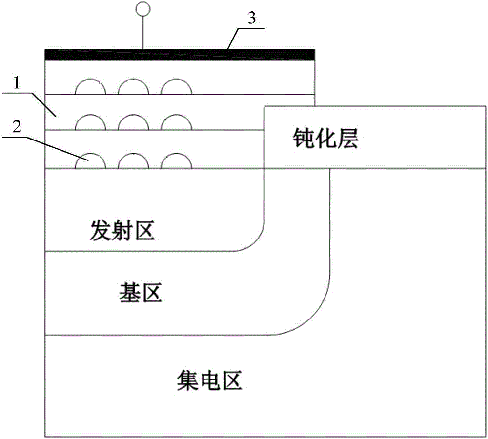
[0022] Specific implementation mode one: refer to figure 2 This implementation mode is described in detail. In this implementation mode, a radiation-resistant bipolar device based on the emitter electrode contact method is described. The metal layer of the bipolar device is connected to the emitter region by using a heterojunction characteristic material to enhance the electrode structure.
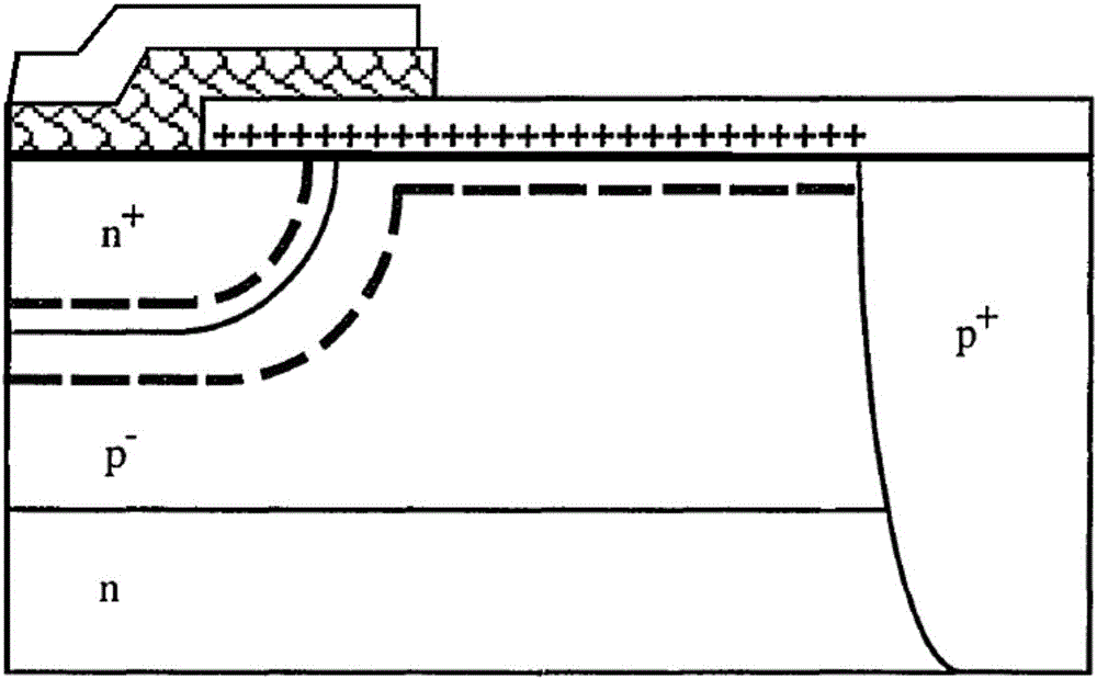
[0023] After bipolar devices (especially NPN bipolar transistors) are damaged by irradiation, the positive charge captured by the oxide will cause the emitter junction (N + P junction) and the depletion layer on the surface of the base region expand to the base region (N-type region), increasing the recombination current in the depletion layer, resulting in the excess base current △I of the bipolar device B (base current minus initial base current after irradiation) increases, which affects the reliability and life of bipolar devices. Schematic diagram of the extended structure of the de...
specific Embodiment approach 2
[0025] Embodiment 2: This embodiment is a further description of the radiation-resistant bipolar device based on the emitter electrode contact method described in Embodiment 1. In this embodiment, the heterojunction characteristic material enhances the electrode The structure includes: polysilicon and metal silicide, the shape of the polysilicon is hemispherical, the metal silicide covers the upper surface of the polysilicon, and the polysilicon contains dopant atoms.
[0026] In this embodiment, a metal compound with excellent conductivity (such as metal silicide) is first formed on the emitter region, and then the metal compound is connected to the emitter region by forming polycrystalline silicon grains, so that the sheet resistance of the improved bipolar device is reduced .
specific Embodiment approach 3
[0027] Specific embodiment three: this embodiment is a further description of the radiation-resistant bipolar device based on the emitter electrode contact method described in specific embodiment two. In this embodiment, the dopant atoms in the polysilicon and The dopant atoms in the emitter region of a bipolar device are of the same type.
[0028] In this embodiment, the dopant atoms in the enhanced electrode structure of the heterojunction material are of the same type as the dopant atoms in the emitter region of the bipolar device. For example, if the emitter region contains N-type dopant atoms, the dopant atoms in the heterojunction characteristic material enhanced electrode structure are also N-type dopant atoms. The reason for using this process is to enhance the emission region and the heterojunction characteristic material. Good electrical conductivity between the electrode structures results.
PUM
 Abstract
Description
Claims
Application Information


