Preparation method of silicon micro-nano hole antireflection texture by utilizing silver nanoparticles to assist secondary etching

A technology of silver nanoparticles and nano-silver particles, which is applied in the direction of final product manufacturing, sustainable manufacturing/processing, electrical components, etc., can solve the problem of single shape, achieve the effect of optimizing the etching structure and improving the effect of anti-reflection

Inactive Publication Date: 2014-06-25
SHAANXI NORMAL UNIV
View PDF8 Cites 7 Cited by
  • Summary
  • Abstract
  • Description
  • Claims
  • Application Information

AI Technical Summary

Problems solved by technology

The current common practice is to use different chemical displacement silver plating methods to deposit Ag particles on silicon substrates as catalysts. 2 o 2 Chemical etching is carried out in the solution, but the etched morphology is single, only the hole structure with adjustable size

Method used


Image

  • Preparation method of silicon micro-nano hole antireflection texture by utilizing silver nanoparticles to assist secondary etching
  • Preparation method of silicon micro-nano hole antireflection texture by utilizing silver nanoparticles to assist secondary etching
  • Preparation method of silicon micro-nano hole antireflection texture by utilizing silver nanoparticles to assist secondary etching

Examples


Embodiment 1

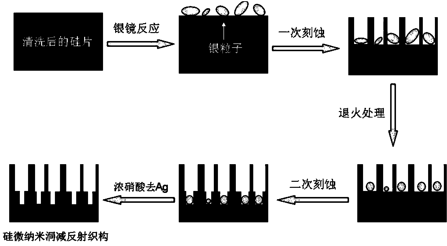
[0029] 1. If figure 1 As shown, at room temperature, the monocrystalline silicon wafer was cleaned with acetone and ethanol for 10 minutes, and then washed with H 2 o 2 with H 2 SO 4 、H 2 The mixed liquid with O volume ratio of 1:3:5 was ultrasonically cleaned for 10 minutes, then rinsed with deionized water and dried with nitrogen gas.

[0030] 2. Immerse the single crystal silicon wafer cleaned in step 1 into AgNO 3 , NaOH, NH 3 ·H 2 In the mixed solution of O, glucose and deionized water, AgNO in the mixed solution 3 The concentration of NaOH is 0.05mol / L, the concentration of NaOH is 0.2mol / L, NH 3 ·H 2 The concentration of O was 1 mol / L, the concentration of glucose was 0.005 mol / L, and the silicon wafer was bathed in 60°C water bath for 4 minutes, so that the surface of the silicon wafer was evenly coated with a layer of nano-silver particles.

[0031] 3. Put the single crystal silicon wafer after silver plating in step 2 into HF10%, H 2 o 2 15%, deionized wa...

Embodiment 2

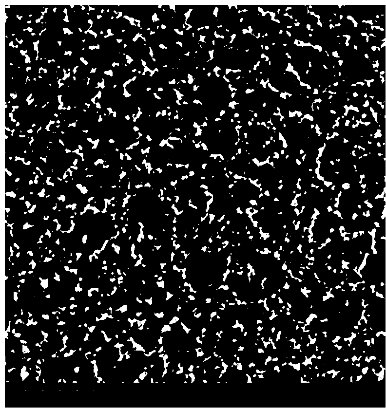
[0041] In step 4 of this embodiment, the monocrystalline silicon wafer etched for the first time is placed in a nitrogen atmosphere, heated to 300° C., kept at a constant temperature for 60 minutes, and then naturally cooled to room temperature. The other steps are the same as in Example 1 to obtain the silicon micro-nano hole anti-reflection texture (see image 3 ).

Embodiment 3

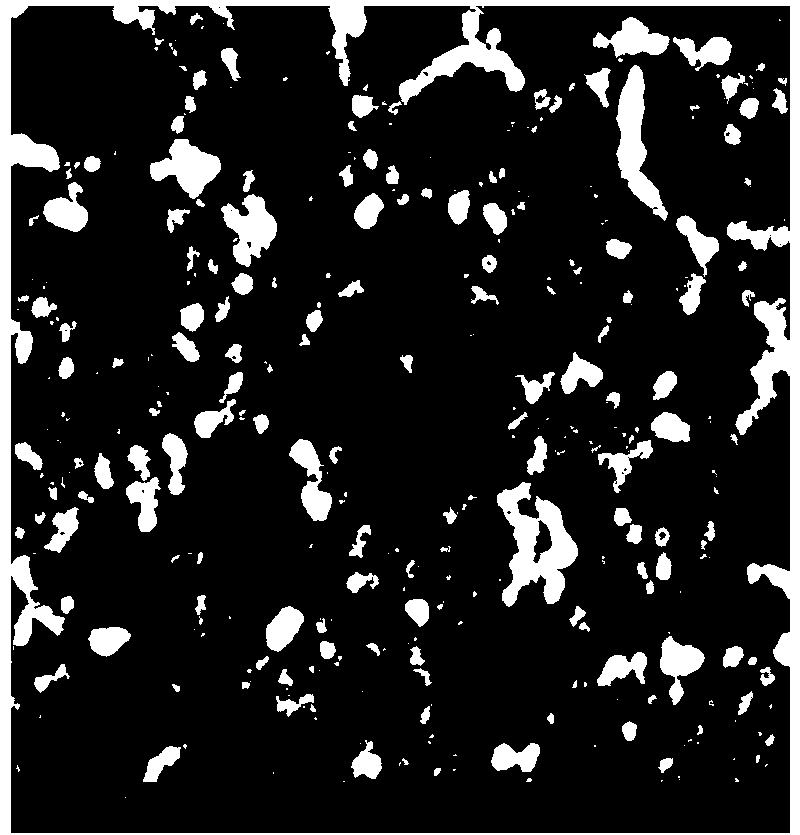
[0043] In Step 4 of this embodiment, the monocrystalline silicon wafer etched for the first time is placed in a nitrogen atmosphere, heated to 500° C., kept at a constant temperature for 60 minutes, and then naturally cooled to room temperature. The other steps are the same as in Example 1 to obtain the silicon micro-nano hole anti-reflection texture (see Figure 4 ).


PUM


Abstract

The invention discloses a preparation method of a silicon micro-nano hole antireflection texture by utilizing silver nanoparticles to assist secondary etching. The preparation method comprises the steps of plating or depositing a layer of silver nanoparticles on a cleaned monocrystalline silicon wafer, preparing the silicon micro-nano hole antireflection texture with large holes through primary etching, performing annealing treatment on the silicon micro-nano hole antireflection texture in an inert atmosphere to enable the silver nanoparticles to become smaller balls, performing secondary etching, forming a layered structure with small holes in the large holes, and removing silver through concentrated nitric acid. Therefore, optimization on an etching structure of a silicon surface is achieved, and antireflection effect of a silicon wafer is improved.

Description

technical field [0001] The invention belongs to the technical field of semiconductor materials, and in particular relates to a method for preparing a silicon micro-nano hole anti-reflection texture. Background technique [0002] Reducing the reflection loss of incident sunlight on the light-receiving surface of a silicon solar cell is one of the effective means to improve the photoelectric conversion efficiency of the cell. Preparation of surface microstructure by noble metal ion-assisted chemical etching of Si is an important means to reduce surface reflectivity. [0003] At present, in the preparation of anti-reflection layer by etching Si with the assistance of noble metal ions, the research of etching Si with Ag particles is the most successful, and the prepared porous layer and Si nanowire array can reduce the surface reflectance to below 10%. , thereby increasing the efficiency of the solar cell. The current common practice is to use different chemical displacement s...

Claims


Application Information

Patent Timeline
IPC IPC(8): H01L31/18H01L31/0236
CPCH01L31/02363H01L31/1804Y02P70/50
Inventor 高斐武怡刘生忠宋飞莺杨勇州王皓石马笑轩
Owner SHAANXI NORMAL UNIV
Why Eureka
Try Eureka