Manufacturing technology of magnetic sensing device

A manufacturing process and magnetic sensing technology, applied in the manufacturing/processing of electromagnetic devices, measuring devices, measuring magnetic variables, etc., can solve the problem of not being able to manufacture three-axis sensors at the same time, and achieve obvious price competitiveness, excellent performance, The effect of good manufacturability

Inactive Publication Date: 2014-06-25
QST CORP
View PDF8 Cites 6 Cited by
  • Summary
  • Abstract
  • Description
  • Claims
  • Application Information

AI Technical Summary

Problems solved by technology

At present, the simultaneous fabrication of three-ax

Method used


Image

  • Manufacturing technology of magnetic sensing device
  • Manufacturing technology of magnetic sensing device
  • Manufacturing technology of magnetic sensing device

Examples


Embodiment 1

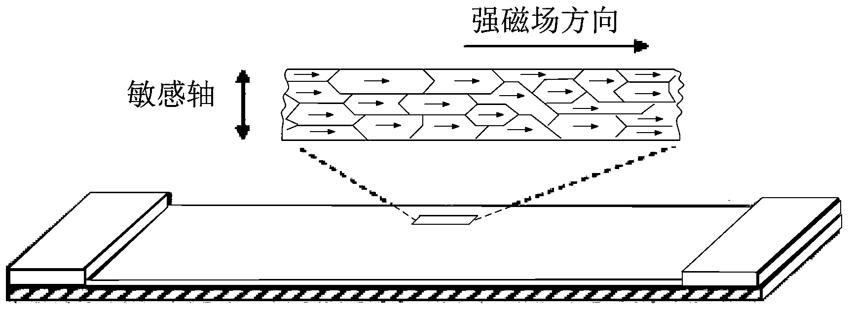
[0069] see Image 6 , Figure 7 ,in, Figure 7 yes Image 6 The projection along the A-A direction; the present invention discloses a magnetic sensing device, which includes a Z-axis magnetic sensing component, and the Z-axis magnetic sensing component includes: a substrate 10, at least one pair of magnetic sensing devices that cooperate Module; the magnetic sensing module includes a magnetic conduction unit 20 and an induction unit. The substrate 10 may include CMOS peripheral circuits. After each pair of matching two magnetic sensing modules is set up, it can directly offset the magnetic field interference of each pair of magnetic sensing modules in the X-axis direction or / and Y-axis direction, and obtain a pure Z-axis signal, so there is no It needs to use peripheral circuits for signal processing, accurate measurement and high precision.

[0070] The surface of the substrate 10 has a dielectric layer, and a groove 11 is opened in the dielectric layer. The substrate i...

Embodiment 2

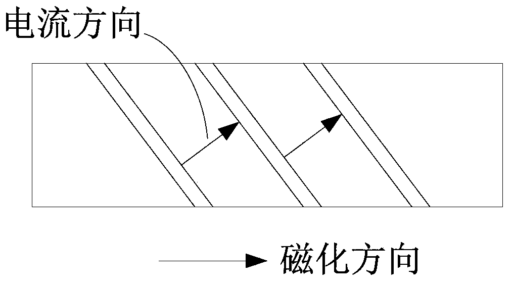
[0105] see Figure 10 The difference between this embodiment and Embodiment 1 is that in this embodiment, the third direction magnetic sensing component includes a first magnetic sensing module 101, a second magnetic sensing module 102, and a third magnetic sensing module 103 , the fourth magnetic sensing module 104 . The magnetic sensing modules are arranged in parallel, or the centers are on the same straight line; that is, the magnetization directions of the magnetic material layers of the sensing units in the magnetic sensing modules are the same or opposite, and the grooves of the magnetic sensing modules are parallel or coincident.

[0106] The first end of the first magnetic sensing module 101 and the first end of the second magnetic sensing module 102 are grounded, and the second end of the first magnetic sensing module 101 is connected to the first end of the fourth magnetic sensing module 104 , the second end of the second magnetic sensing module 102 is connected to...


PUM


Abstract

The invention discloses a manufacturing technology of a magnetic sensing device. The technology comprises steps of depositing dielectric material on a substrate to form a dielectric material layer, opening a groove in the dielectric material layer, depositing a second dielectric material layer on the dielectric material layer, depositing magnetic material and electrode material respectively on the second dielectric material layer to form a deposition magnetic material layer and an electrode material layer respectively, depositing photoresist and carrying out exposal and development, carrying out etching to remove partial magnetic material and electrode material, removing the photoresist, depositing third dielectric material, removing partial third dielectric material through etching and retaining dielectric material only at corners to form a dielectric material side wall protection layer, depositing second electrode material on the magnetic material layer of the sensing unit and carrying out photoetching to form a second electrode, and filling dielectric material, carrying out planarization in match with chemical mechanical polishing, and leading out the second electrode through the semiconductor technology. the manufacturing technology of the magnetic sensing device provided by the invention can manufacture a three-axis magnetic induction device on the same wafer or chip.

Description

technical field [0001] The invention belongs to the technical field of semiconductor technology and relates to a magnetic sensing device, in particular to a manufacturing process of the magnetic sensing device. Background technique [0002] According to its principle, magnetic sensors can be divided into the following categories: Hall elements, magneto-sensitive diodes, anisotropic magnetoresistance elements (AMR), tunnel junction magnetoresistance (TMR) elements and giant magnetoresistance (GMR) elements, induction coils , superconducting quantum interference magnetometer, etc. [0003] Electronic compass is one of the important application fields of magnetic sensors. With the rapid development of consumer electronics in recent years, in addition to navigation systems, more and more smart phones and tablet computers have also begun to be equipped with electronic compass as standard, bringing users In recent years, the demand for magnetic sensors has also begun to develop f...

Claims


Application Information

Patent Timeline
IPC IPC(8): H01L43/12G01R33/09
Inventor 不公告发明人
Owner QST CORP
Why Eureka
Try Eureka