

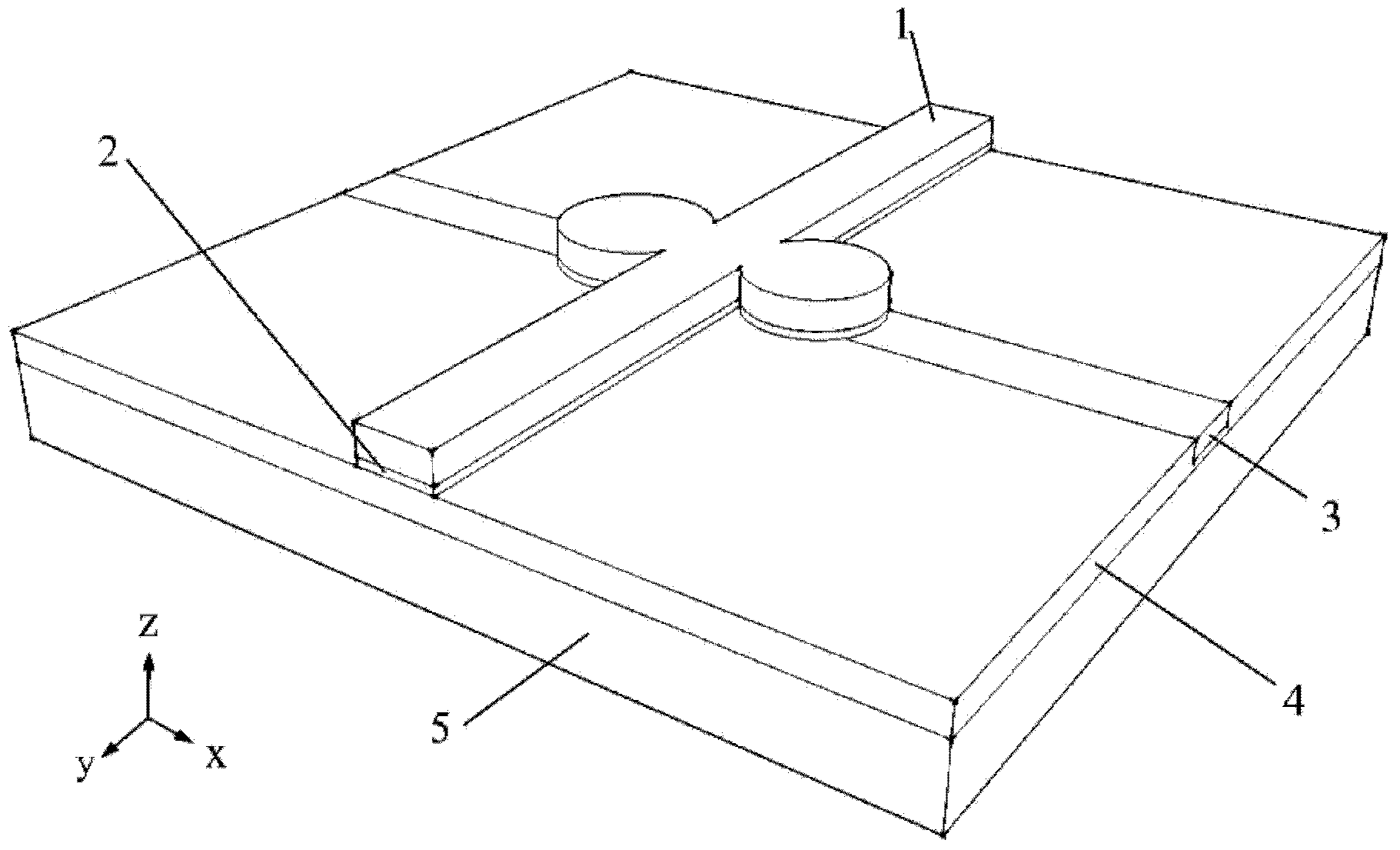
Electric injection surface plasma micro-nano structure waveguide output laser source of coplanar electrode
A surface plasmon, coplanar electrode technology, applied in phonon exciters, circuits, electrical components, etc., can solve problems such as external
- Summary
- Abstract
- Description
- Claims
- Application Information
AI Technical Summary
Problems solved by technology
Method used
Image

Examples
Embodiment 1
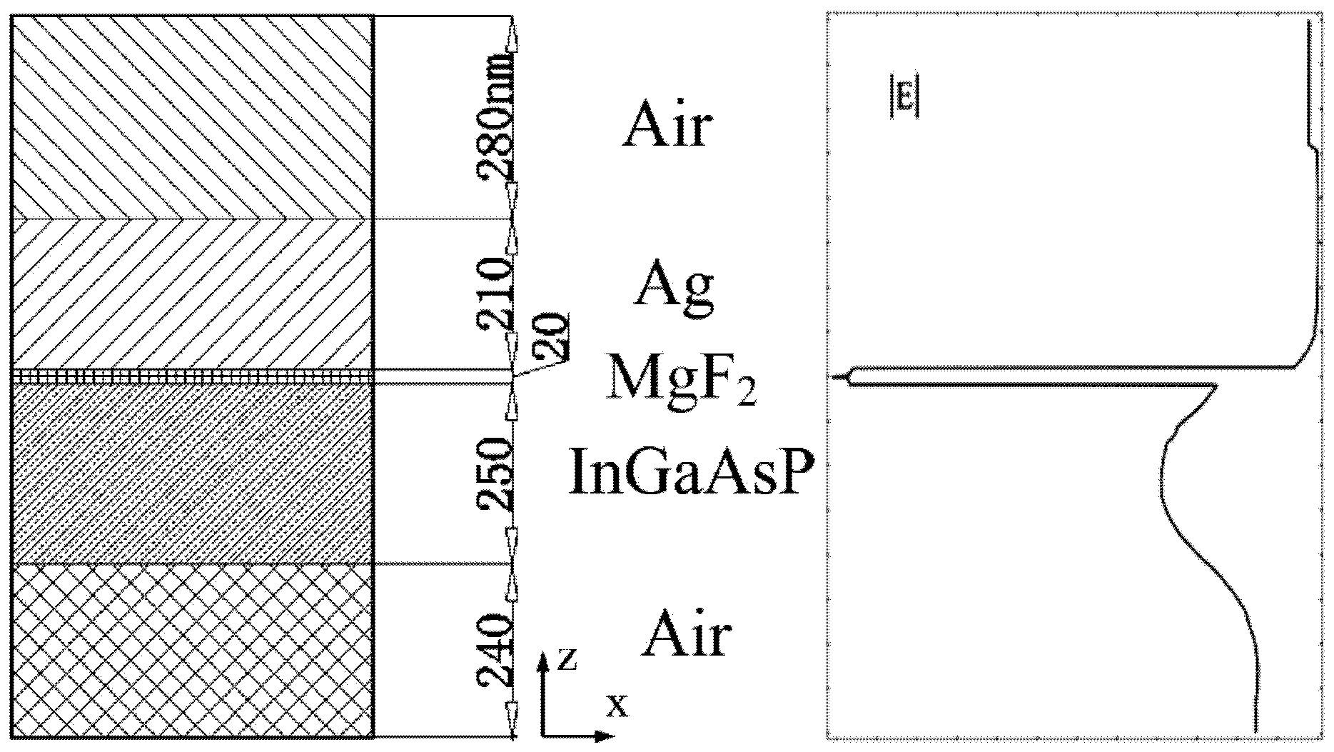
[0037] In this embodiment, the semiconductor active material and the two circular ion implantation regions adopt InGaAsP multiple quantum well material with a refractive index of 3.3, a thickness of 205nm and a waveguide width of 1500nm; the metal is Ag with a refractive index of 0.514-10.8i, and the The thickness is 250nm, the width of the silver strip is 1500nm; the insulating layer is MgF 2 The refractive index is 1.38 and the thickness is 20nm.
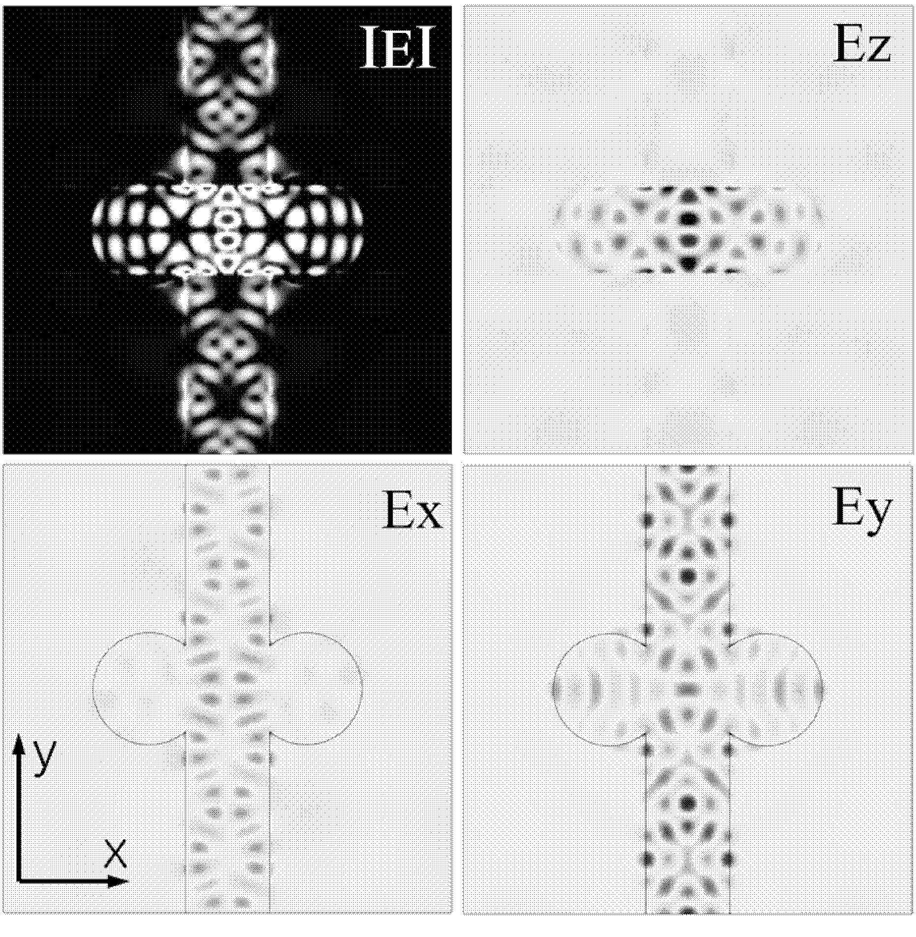
[0038] In this example, the COMOSL3D Eigenfrequency module is used for simulation experiments. Here we use air instead of figure 1 Middle area 4 and 5, in order to simplify the calculation amount of the simulation experiment, the parameters are set as above. The electric field along the depth Z direction in the subwavelength cavity is strongly confined to 20nm MgF 2 layer, such as figure 2 As shown, surface plasmon resonance is formed. The distribution of the electric field and its components in the simulation results is as f...
PUM
| Property | Measurement | Unit |
|---|---|---|
| Thickness | aaaaa | aaaaa |
| Thickness | aaaaa | aaaaa |
| Thickness | aaaaa | aaaaa |
Abstract
Description
Claims
Application Information