Two-dimensional silicon-based micro-nano photonic crystal solar cell

A solar cell and micro-nano photonic technology, applied in the field of solar cells, can solve the problems of the combination of no band gap and slow light theory, the high cost of anti-reflection film preparation, the difficult control of the preparation process, etc., so as to increase the photoelectric conversion efficiency and improve the electrical Transmission performance, coupling of light and effect of high transmission efficiency

Inactive Publication Date: 2014-12-24
QINGDAO UNIV
View PDF4 Cites 5 Cited by
  • Summary
  • Abstract
  • Description
  • Claims
  • Application Information

AI Technical Summary

Problems solved by technology

[0004] (2) Gradient refractive index anti-reflection coating is an anti-reflection coating with a gradually changing refractive index deposited on the surface of silicon. It can achieve very low reflectivity in a wide spectrum and a wide range of incident angles. The preparation cost is high, and it is difficult to find materials that meet the requirements of the refractive index;
[0005] (3) Suede anti-reflection film is a combination of anti-reflection film technology and surface texturing technology to prepare anti-reflection film with suede structure, so as to realize the function of 1 / 4 wavelength anti-reflection film, and at the same time change and reduce reflection The rate increases with the increase of the incident angle, but this kind of anti-reflection film needs the combination of physical, chemical and even microelectronic methods, and the preparation process is difficult to control, so most of the research is in the experimental stage
[0006] Recently, studies have suggested that silicon nanowires (or silicon pores) may be one of the most potential, low-cost, and high-efficiency solar cell device materials. Silicon nanowires can increase light absorption, and have carriers that only need to diffuse a short distance. It can achieve the advantages of the junction area, but the existing research is mostly on the one-dimensional structure of the nano-solar cell structure, and the mechanism used is also to trap light through diffuse reflection. Some studies have proposed a two-dimensional structure of radial silicon nanowires, but the manufacturing process is complicated. Also not combined with the forbidden band and slow light theory of photonic crystal structure

Method used


Image

  • Two-dimensional silicon-based micro-nano photonic crystal solar cell
  • Two-dimensional silicon-based micro-nano photonic crystal solar cell
  • Two-dimensional silicon-based micro-nano photonic crystal solar cell

Examples


Embodiment 1

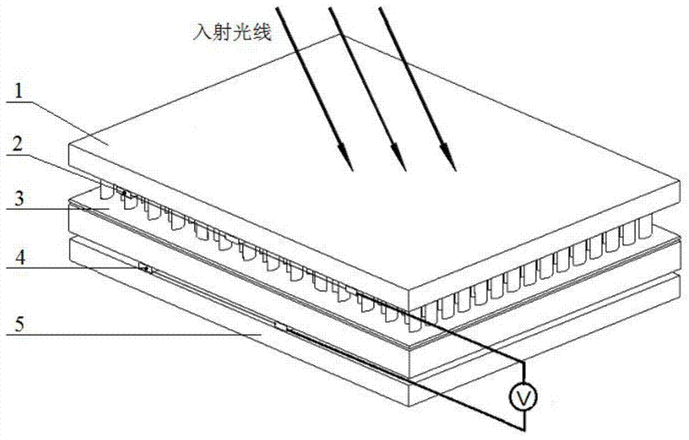
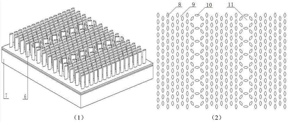
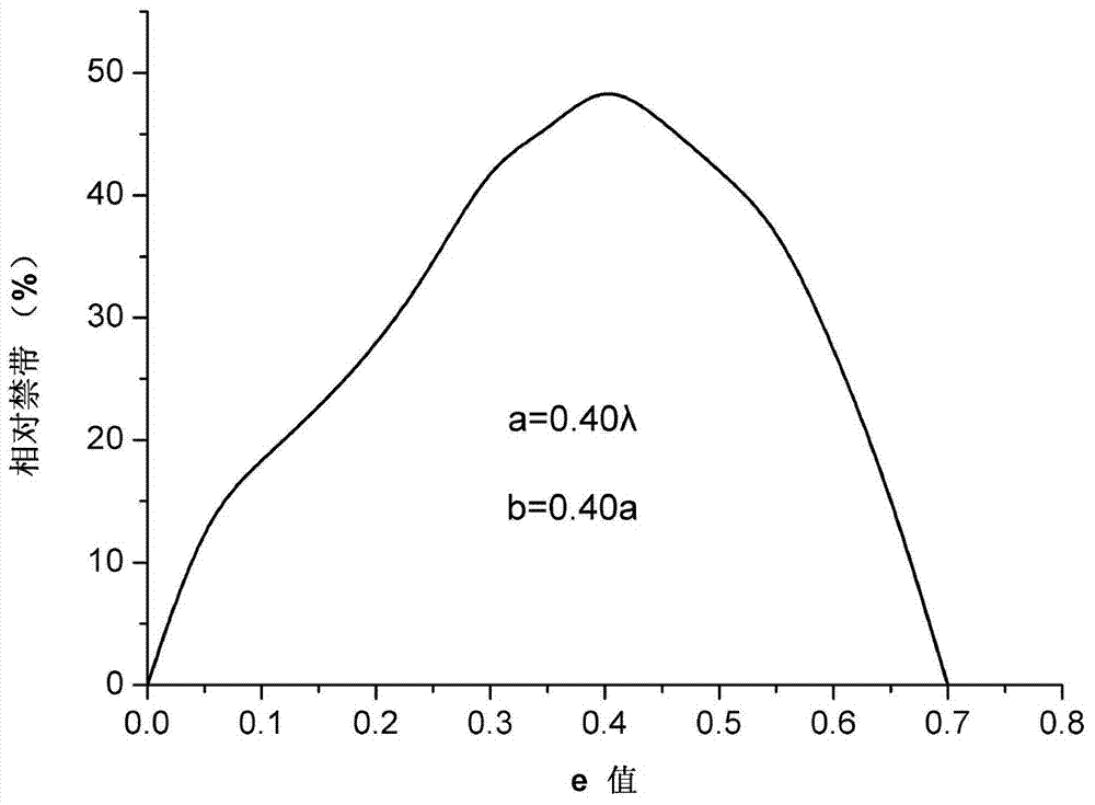
[0033] The overall structure of this embodiment is as figure 1 As shown, the n-type silicon semiconductor 6 involved in the two-dimensional silicon-based micro-nano photonic crystal solar cell structure 3 is a structure with two substructures of forbidden band and slow light effect arranged periodically, and the scattering element of the n-type silicon semiconductor 6 adopts Circular segment, spatially arranged as a triangular lattice structure; the central wavelength of the forbidden band is set at λ=700nm, which can be obtained by the plane wave expansion method: when the central wavelength of the forbidden band is set at 700nm, the lattice constant of the structure is a=0.4 When λ=280nm, parameters b=0.4a, e=0.4, both the forbidden band and slow light have better effects; since the forbidden band of the structure is close to 50% of the central wavelength, such as image 3 As shown, the forbidden band of such a structure is between 350 and 1050nm, and this range includes not...

Embodiment 2

[0036] The overall structure of this embodiment and figure 1 same. The upper layer n-type silicon semiconductor 6 in the two-dimensional silicon-based micro-nano photonic crystal solar cell structure 3 involved in the embodiment is a structure with two substructures of forbidden band and slow light effect arranged periodically. In order to meet the large forbidden band of the structure, the scattering element adopts a circular bow shape; the spatial arrangement of the structure is a triangular lattice structure; the central wavelength of the forbidden band is set at λ=700nm, which can be obtained by the plane wave expansion method: When the central wavelength of the structure is set at 700nm, the lattice constant of the structure is a=0.375λ=262.5nm, and when the parameters b=0.42a, e=0.3, the forbidden band and slow light also have good effects; because the forbidden band of the structure is close to 43% of the center wavelength, as Figure 7 As shown, the forbidden band of...


PUM


Abstract

The invention belongs to the technical field of solar cells, and relates to a two-dimensional silicon-based micro-nano photonic crystal solar cell. The two-dimensional silicon-based micro-nano photonic crystal solar cell is characterized in that front electrodes which are periodically arrayed are arranged on the lower side surface of a front contact layer; a two-dimensional silicon-based micro-nano photonic crystal solar cell structure is arranged between the front electrodes and back electrodes, upper layers of the two-dimensional silicon-based micro-nano photonic crystal solar cell structure are type-n silicon semiconductor layers, a lower layer of the two-dimensional silicon-based micro-nano photonic crystal solar cell structure is a type-p silicon semiconductor layer, and PN junctions are formed by the type-n silicon semiconductor layers and the type-p silicon semiconductor layer; a back contact layer is arranged at the bottoms of the back electrodes, and the back contact layer and the front contact layer are made of identical materials; the back electrodes which are of aluminum thin layer structures are arranged in slow-light regions or band-gap regions of the type-p silicon semiconductor layer. The two-dimensional silicon-based micro-nano photonic crystal solar cell has the advantages that the two-dimensional silicon-based micro-nano photonic crystal solar cell is simple in structure, small in size, low in threshold, short in carrier diffusion distance and high in stability, light coupling efficiency and light transmission efficiency, is far thinner than the traditional silicon solar cell and becomes a new-generation low-cost and efficient solar cell device with the maximum potential, and mature processing and composite technologies are implemented.

Description

Technical field: [0001] The invention belongs to the technical field of solar cells, and relates to a novel photonic crystal solar cell structure, in particular to a two-dimensional silicon-based micro-nano photon with photonic band gap and slow light effect, small thickness, good light trapping, and high photoelectric conversion efficiency Crystalline solar cells. Background technique: [0002] Solar cells are semiconductor devices that convert light energy into electrical energy. Batteries, organic thin-film solar cells and fuel-sensitized solar cells, silicon-based solar cells are widely used at present, because silicon raw materials are abundant, photoelectric conversion efficiency is high, photoelectric performance stability and reliability are high, and processing technology is mature. It does not contain toxic elements, does not cause pollution to the environment, and is determined by factors such as high market acceptance. The main factors affecting the efficiency ...

Claims


Application Information

Patent Timeline
Patent Type & Authority Applications(China)
IPC IPC(8): H01L31/055H01L31/054
CPCY02E10/52H01L31/035209H01L31/022441
Inventor 万勇刘培晨韩文娟贾明辉孙蕾
Owner QINGDAO UNIV
Why Eureka
Try Eureka