Heat sink used for downward encapsulation of p side of semiconductor laser unit and manufacturing method thereof
A technology of lasers and semiconductors, which is applied in the direction of semiconductor lasers, lasers, laser components, etc., can solve the problems of difficult p-side down packaging, etc., and achieve the effects of easy integration, extended life, and enhanced heat dissipation
- Summary
- Abstract
- Description
- Claims
- Application Information
AI Technical Summary
Problems solved by technology
Method used
Image

Examples
Embodiment 1
[0034] The specific implementation process of embodiment one includes:
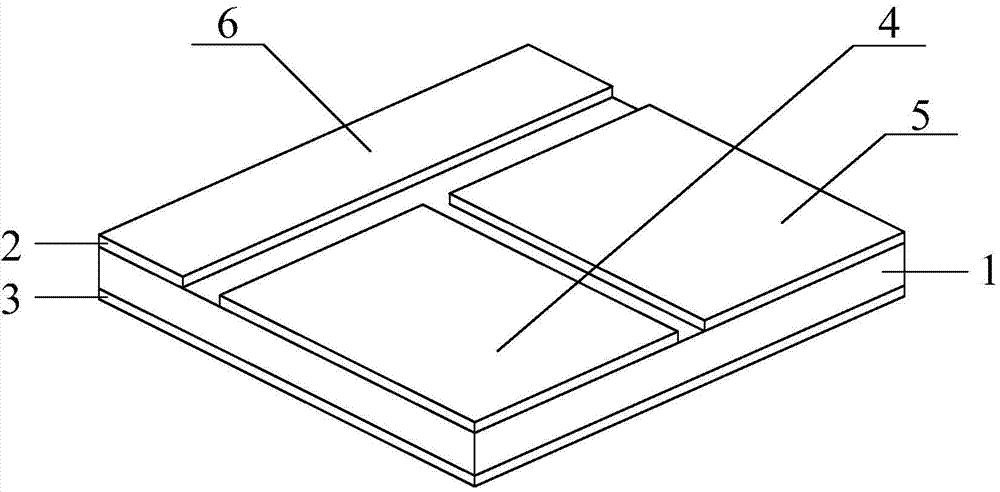
[0035] Step 1, prepare the base material layer 1, and grow the upper metal layer 2 and the lower metal layer 3 respectively on the upper and lower surfaces of the base material layer 1, and the side of the base material layer 1 is not coated with a metal layer, so as to ensure that the upper metal layer 2 and the lower metal layer There is an open circuit between the metal layers 3.
[0036] Step 2, preparing an insulating isolation groove, and separating the upper metal layer 2 into independent first positive electrode 4, second positive electrode 5 and negative electrode 6 through the insulating isolation groove;
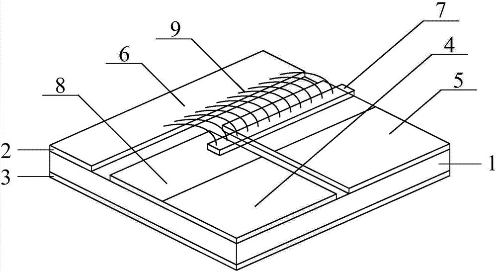
[0037] Step 3, solder layer 8 is plated on the first positive electrode 4 and the second positive electrode 5, the first positive electrode 4 is connected with the ridge waveguide region of the semiconductor laser 7 through the solder layer 8, and the second positive electrode 5 is passed thr...
Embodiment 2
[0040] The second embodiment is based on the first embodiment, specifically a method of packaging the p-side down of a GaAs-based p-electrode separation semiconductor laser chip. It uses silicon nitride ceramics as the material of the base material layer, and the size of the base material layer is 5.5mm×4.5mm×1mm, and the upper metal layer and the lower metal layer use titanium gold, titanium platinum gold or gold germanium nickel with a total thickness of 1um. Gold, and use the solder layer of gold-tin material to sinter the p-electrode separation semiconductor laser chip p-side down on the heat sink. The implementation process mainly includes the following steps:
[0041] Step A, using the method of magnetron sputtering, sputtering titanium gold, titanium platinum gold or gold germanium nickel gold with a thickness of 1um on the upper and lower surfaces of the silicon nitride ceramic base material layer as the metal layer, and the side of the base material layer is not plated...
PUM
 Abstract
Description
Claims
Application Information
 - Generate Ideas
- Intellectual Property
- Life Sciences
- Materials
- Tech Scout
- Unparalleled Data Quality
- Higher Quality Content
- 60% Fewer Hallucinations
Browse by: Latest US Patents, China's latest patents, Technical Efficacy Thesaurus, Application Domain, Technology Topic, Popular Technical Reports.
© 2025 PatSnap. All rights reserved.Legal|Privacy policy|Modern Slavery Act Transparency Statement|Sitemap|About US| Contact US: help@patsnap.com