Ultra-high-definition CMOS image sensor pixel circuit of three-dimensional structure and method for controlling ultra-high-definition CMOS image sensor pixel circuit of three-dimensional structure

An image sensor and pixel circuit technology, applied in the field of image sensing, can solve the problems that the image signal transmission speed and analog-to-digital conversion speed cannot keep up with the image signal reading speed, and the signal noise is high, so as to increase the aperture ratio and improve the image quality , Improve the effect of analog-to-digital conversion speed

Inactive Publication Date: 2014-07-02
BEIJING INST OF COMP TECH & APPL +1
View PDF7 Cites 23 Cited by
  • Summary
  • Abstract
  • Description
  • Claims
  • Application Information

AI Technical Summary

Problems solved by technology

However, one of the aspects that currently restricts the development of image sensor chip performance is that the transmission speed and analog-to-digital conversion speed of the image signal cannot keep up with the reading speed of the image signal, and at the same time, the signal noise of the readout is relatively high.

Method used


Image

  • Ultra-high-definition CMOS image sensor pixel circuit of three-dimensional structure and method for controlling ultra-high-definition CMOS image sensor pixel circuit of three-dimensional structure
  • Ultra-high-definition CMOS image sensor pixel circuit of three-dimensional structure and method for controlling ultra-high-definition CMOS image sensor pixel circuit of three-dimensional structure
  • Ultra-high-definition CMOS image sensor pixel circuit of three-dimensional structure and method for controlling ultra-high-definition CMOS image sensor pixel circuit of three-dimensional structure

Examples


Embodiment Construction

[0058] The technical solution of the present invention will be described in detail below in conjunction with the accompanying drawings and specific embodiments to further understand the purpose, solution and effect of the present invention, but it is not intended to limit the scope of protection of the appended claims of the present invention.

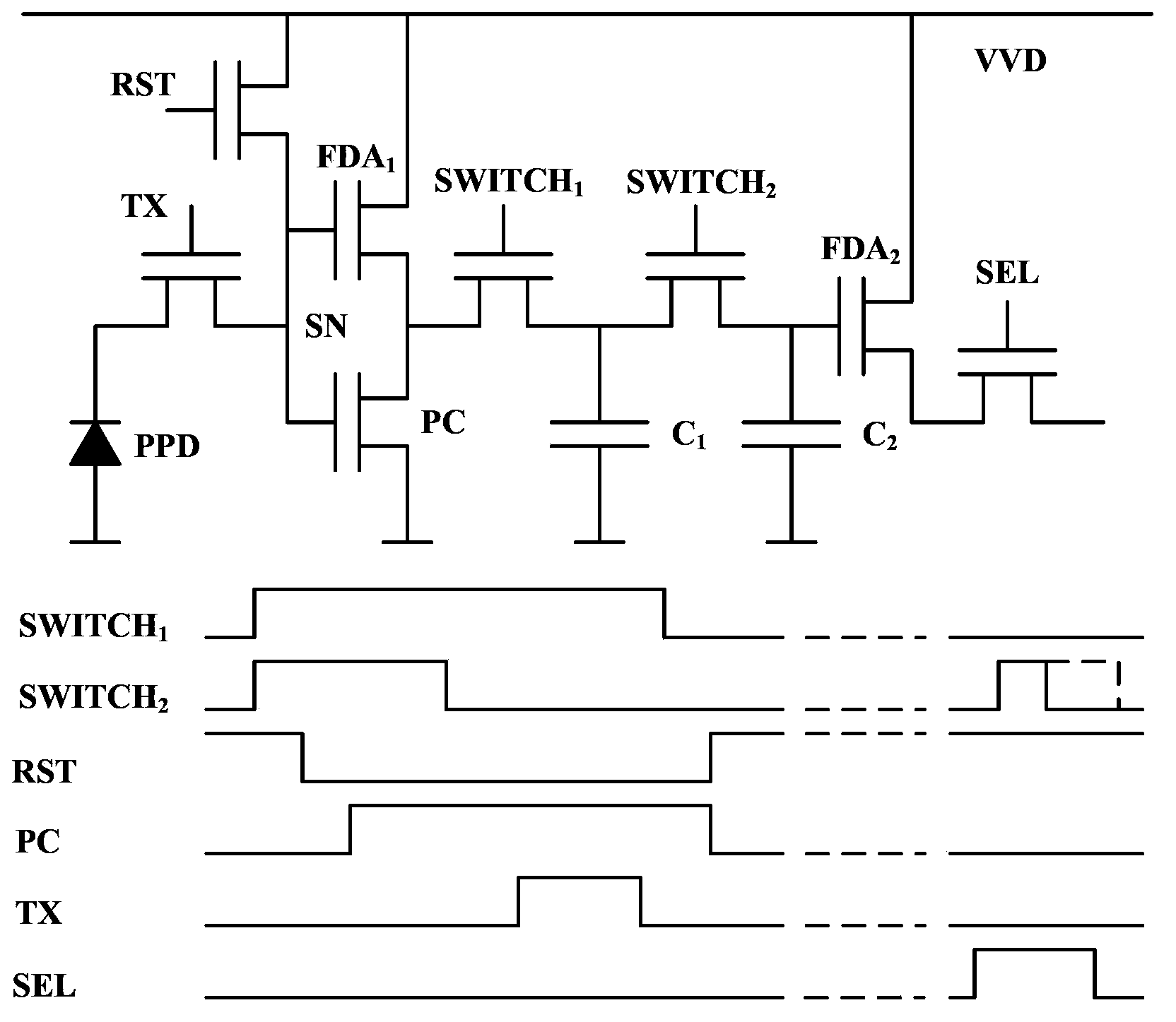
[0059] like figure 1 Shown is the pixel circuit diagram of the ultra-high-definition CMOS image sensor of the three-dimensional structure of the present invention.

[0060] exist figure 1 In, the pixel circuit consists of reset transistor RST, transfer transistor TX, bias transistor PC, switch transistor SWITCH 1 、SWITCH 2 (abbreviated SW), Floating Diffusion Amplifier FDA 1 、FDA 2 , the selection transistor SEL consists of 8 transistors in total. In addition, there are photodiodes PPD and two sampling capacitors C 1 、C 2 .

[0061] The photodiode PPD is directly connected to the transmission transistor TX, and the transmission...


PUM


Abstract

The invention discloses an ultra-high-definition CMOS image sensor pixel circuit of a three-dimensional structure and a method for controlling the ultra-high-definition CMOS image sensor pixel circuit of the three-dimensional structure. The pixel circuit comprises a photosensitive element, a sensing node, a transmission transistor, a reset transistor, a selection transistor, a first floating diffusion amplifier, a second floating diffusion amplifier, a first sampling capacitor, a second sampling capacitor, a first switch transistor and a second switch transistor, wherein the second floating diffusion amplifier conducts sampling on the voltage in a second sampling capacitor, so that a first sampling signal and a second sampling signal are obtained, and correlated double sampling is conducted on the first sampling signal and the second sampling signal through an analog-digital conversion circuit, so that an image signal is obtained. According to the ultra-high-definition CMOS image sensor pixel circuit of the three-dimensional structure and the method for controlling the ultra-high-definition CMOS image sensor pixel circuit of the three-dimensional structure, an overall shutter is obtained with low noise in an ultra-high-definition CMOS image sensor, and high-speed conversion and transmission of the image signal are achieved.

Description

technical field [0001] The invention relates to the field of image sensing, in particular to the layout improvement of a pixel circuit of a CMOS image sensor and a high-speed readout method of a pixel array signal for ultra-high-definition requirements. Background technique [0002] Image sensors are usually implemented by charge-coupled technology (CCD) and complementary metal-oxide-semiconductor technology (CMOS). CMOS image sensor chip technology uses the photoelectric effect of complementary metal oxide semiconductors to realize the electrical signal conversion of optical signals through photosensitive diode arrays, thus endowing the general integrated circuit chip with the ability to perceive external images. CMOS image sensors are compatible with modern semiconductor industry production processes. The vast majority of integrated circuit chips are manufactured using low-resistivity semiconductor materials and processes, while traditional CCDs use high-resistivity wafer...

Claims


Application Information

Patent Timeline
Patent Type & Authority Applications(China)
IPC IPC(8): H04N5/374H04N5/365H04N5/3745H04N5/378H01L27/146
Inventor 苏威积钟松延吕英全春来申屠燕东范雄涛王雅云谢小权申世光袁晓光叶东升王清理任强黄敏君陈攀裴彦杰何毅白松林秀春赵薇董博徐学淼张力杜丽孟飞张春杰黄传鹤
Owner BEIJING INST OF COMP TECH & APPL
Why Eureka
Try Eureka