Method for reducing ohmic contact resistance of HEMT device

A technology of ohmic contact and devices, applied in semiconductor devices, semiconductor/solid-state device manufacturing, circuits, etc., can solve problems such as unsatisfactory surface morphology and edge uniformity, and GaN material damage

Inactive Publication Date: 2014-07-16
THE 13TH RES INST OF CHINA ELECTRONICS TECH GRP CORP
View PDF6 Cites 4 Cited by
  • Summary
  • Abstract
  • Description
  • Claims
  • Application Information

AI Technical Summary

Problems solved by technology

However, judging from the existing results, the above-mentioned methods all require high-temperature alloys, and the surface morphology and edge regularity after alloying are not ideal and need to be improved.
In addition, there is also ion implantation through the source and drain regions to achieve low ohmic contact and good surface morphology, but this process requires high temperature to activate the implanted ions, and there will be lateral diffusion during the implantation process, causing damage to the GaN material

Method used


Image

  • Method for reducing ohmic contact resistance of HEMT device
  • Method for reducing ohmic contact resistance of HEMT device
  • Method for reducing ohmic contact resistance of HEMT device

Examples


Embodiment 1

[0038] In this embodiment, the AlGaN / GaN HEMT device material is taken as an example, and the embodiments of the present invention are described in detail with reference to the accompanying drawings:

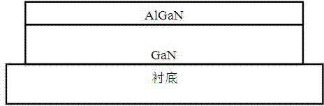
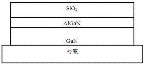
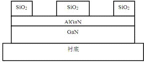
[0039] figure 1 It is a schematic diagram of the structure of AlGaN / GaN HEMT device materials after step 1); 150nm silicon dioxide (SiO 2 ),Such as figure 2 Shown; use reactive ion etching equipment (RIE) to etch SiO in the source and drain ohmic regions of HEMT devices 2 Layer to the upper surface of the AlGaN barrier layer, such as image 3 As shown, the above steps can be implemented by existing technology.

[0040] The invention of the present invention lies in the use of inductively coupled plasma etching equipment (ICP) to etch the source and drain ohmic regions of the HEMT device after the GaN is etched and before the secondary epitaxial growth of n-type heavily doped GaN, the thermal rapid annealing equipment is used to remove the above materials Low-temperature annealing tr...

Embodiment 2

[0044] In this embodiment, the InAlN / GaN HEMT device material is taken as an example to illustrate the implementation of the present invention in detail:

[0045] Grow 200nm silicon dioxide on the surface of InAlN / GaN material (SiO 2 ) Layer; use reactive ion etching equipment (RIE) to etch SiO in the source and drain ohmic regions 2 Layer to the upper surface of the InAlN barrier layer; use inductively coupled plasma etching equipment (ICP) to etch the GaN material in the source and drain ohmic regions of the HEMT device, and etch below the InAlN / GaN heterojunction interface (the etching depth is about 50nm ), and then use a high-temperature annealing furnace to anneal the above devices in a pure nitrogen atmosphere (other protective gases can also be used) or a vacuum atmosphere. The annealing temperature is 300°C and the time is 3 minutes; the MOCVD equipment is used to process the above devices The source and drain ohmic region of the second epitaxy 60nm n-type heavily doped G...

Embodiment 3

[0047] In this embodiment, the InAlN / GaN HEMT device material is taken as an example to illustrate the implementation of the present invention in detail. The focus of this embodiment is on the adjustment of process parameters:

[0048] Grow 200nm silicon dioxide on the surface of InAlN / GaN material (SiO 2 ) Layer; use reactive ion etching equipment (RIE) to etch SiO in the source and drain ohmic regions 2 Layer to the upper surface of the InAlN barrier layer; use inductively coupled plasma etching equipment (ICP) to etch the GaN material in the source and drain ohmic regions of the HEMT device, and etch below the InAlN / GaN heterojunction interface (the etching depth is about 40nm ), and then use a high-temperature annealing furnace to anneal the above-mentioned devices in a pure nitrogen atmosphere (other protective gases can also be used) or a vacuum atmosphere. The annealing temperature is 800°C and the time is 0.5 minutes; the MOCVD equipment is used to process the above-mention...


PUM

PropertyMeasurementUnit
thicknessaaaaaaaaaa
thicknessaaaaaaaaaa

Abstract

The invention discloses a method for reducing the ohmic contact resistance of an HEMT device, and relates to the technical field of nitride preparation methods. The method comprises the following steps that (1) epitaxial structure growth is carried out, and a GaN layer and a barrier layer are formed on a substrate in sequence; (2) a SiO2 layer is grown on the upper surface of the barrier layer; (3) the SiO2 layer is etched in a drain and source ohmic area to the upper surface of the barrier layer; (4) etching is carried out on a GaN material in the drain and source ohmic area to the position below a heterojunction interface between the GaN layer and the barrier layer, and then a high-temperature annealing furnace is used for carrying out annealing treatment in a pure nitrogen atmosphere or a vacuum atmosphere; (5) secondary epitaxy of an n-type heavy doping GaN material is carried out in the drain and source ohmic area; (6) residual SiO2 on the upper surface of the barrier layer is removed through corrosion. According to the method for reducing the ohmic contact resistance of the HEMT device, ohmic contact between n-type heavy doping GaN and the side wall of a GaN heterojunction is improved, and the contact resistance between the n-type heavy doping GaN and the side wall of the GaN heterojunction is reduced.

Description

Technical field [0001] The invention relates to the technical field of preparation methods of nitrides, and in particular to a method for reducing the ohmic contact resistance of HEMT devices. Background technique [0002] As a representative of the third generation of semiconductor materials, GaN material is an important semiconductor material after Si and GaAs materials. Due to its large forbidden band width, high critical field strength, high carrier saturation velocity, high temperature and radiation resistance The excellent characteristics such as photos have received widespread attention. Among them, the excellent performance of GaN-based heterojunctions (such as AlGaN / GaN and InAl / GaN) high electron mobility field effect transistors (HEMT) in the microwave and millimeter wave fields has made them extensive and in-depth at home and abroad Through the efforts of recent years, the performance and stability of GaN-based HEMT devices have been greatly improved. [0003] In the ...

Claims


Application Information

Patent Timeline
Patent Type & Authority Applications(China)
IPC IPC(8): H01L21/335
CPCH01L29/66462H01L21/28H01L29/401
Inventor 吕元杰冯志红王元刚徐鹏尹甲运敦少博
Owner THE 13TH RES INST OF CHINA ELECTRONICS TECH GRP CORP
Why Eureka
Try Eureka