Non-outer-pin packaging structure and manufacturing method and wire frame of non-outer-pin packaging structure

A technology of a lead frame and a manufacturing method, which is applied in semiconductor/solid-state device manufacturing, semiconductor devices, semiconductor/solid-state device components, etc., can solve the problems of plastic packaging material detaching from pins and easy loss of cutting tools, etc., so as to improve reliability, Improve the cutting rate and prevent loss

Inactive Publication Date: 2014-07-16
SILERGY SEMICON TECH (HANGZHOU) CO LTD
View PDF6 Cites 11 Cited by
  • Summary
  • Abstract
  • Description
  • Claims
  • Application Information

AI Technical Summary

Problems solved by technology

[0005] In view of this, the purpose of the present invention is to provide an improved leadless package structure and its manufacturing method and lead frame to solve the problem that the leadless package structure in the prior art causes the cutting tool to be easily worn out and easily caused during the cutting process. The problem that the plastic encapsulant is detached from the pin

Method used


Image

  • Non-outer-pin packaging structure and manufacturing method and wire frame of non-outer-pin packaging structure
  • Non-outer-pin packaging structure and manufacturing method and wire frame of non-outer-pin packaging structure
  • Non-outer-pin packaging structure and manufacturing method and wire frame of non-outer-pin packaging structure

Examples


Embodiment Construction

[0046] The leadless package structure proposed by the present invention, its manufacturing method and lead frame will be further described in detail below with reference to the accompanying drawings and specific embodiments. Advantages and features of the present invention will be apparent from the following description and claims. It should be noted that all the drawings are in a very simplified form and use imprecise scales, and are only used to facilitate and clearly assist the purpose of illustrating the embodiments of the present invention.

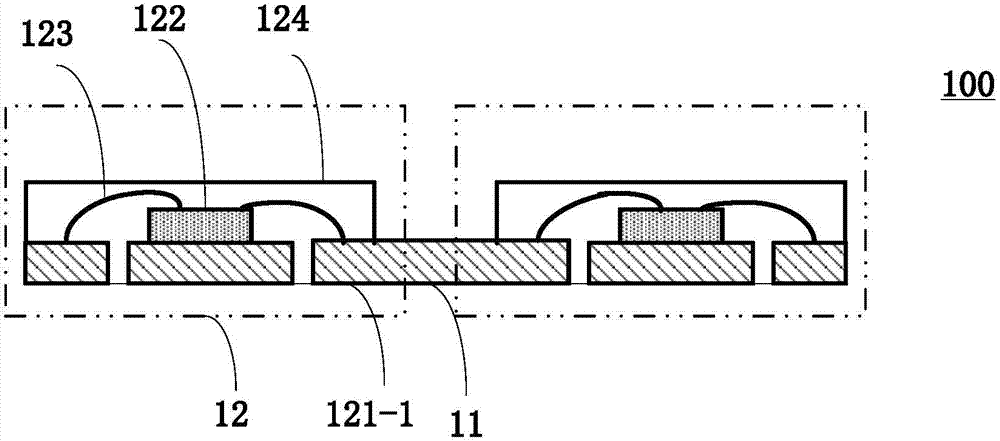
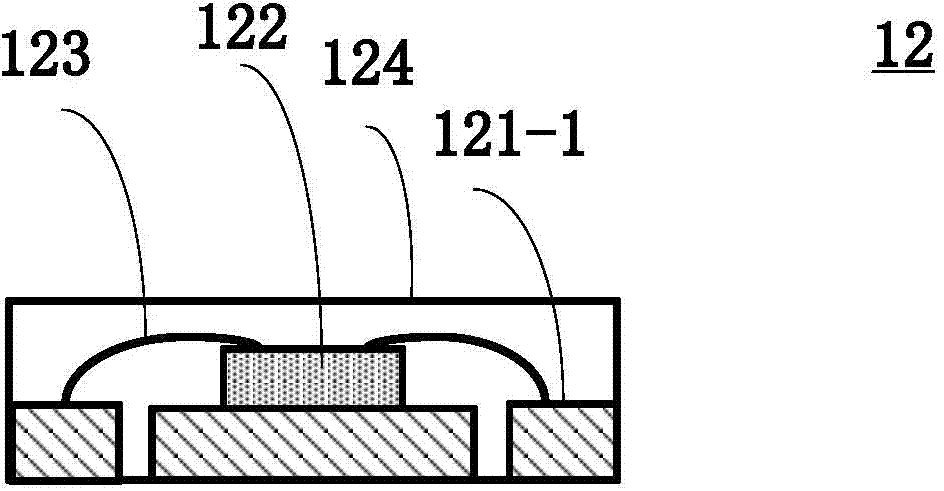
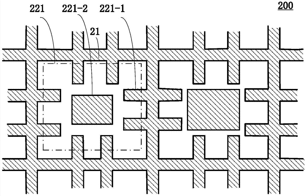
[0047] Please refer to Figure 2A and Figure 2BAs shown, the lead frame 200 of the leadless packaging structure according to an embodiment of the present invention can generally be formed by etching, stamping or other processes of metal plate materials such as copper, aluminum or alloys, and mainly includes: several connecting brackets 21, several lead frame unit 221. The plurality of connecting brackets 21 are arranged in a stag...


PUM


Abstract

The invention provides a non-outer-pin packaging structure and a manufacturing method and a wire frame of the non-outer-pin packaging structure. The non-outer-pin packaging structure comprises the wire frame, a chip, a plurality of electric connection elements and a plastic packaging body. The wire frame comprises a wire frame unit and a connecting support. The wire frame unit comprises a plurality of pins connected with the connecting support, and the thickness of the ends, away from the wire frame unit, of the pins is smaller than the thickness of the pins. The chip is electrically connected to the pins through the electric connection elements. The plastic packaging body packages the chip and the electric connection elements and encapsulates the pins. The ends, away from the center of the wire frame unit, of the pins can have first parts with the thickness smaller than that of the pins, one side of each first part is a cutting channel, the metal thickness at the cutting positions is reduced, the loss of a cutter can be reduced, the cutting efficiency can be improved, the contact area between the pins and plastic packaging materials is increased, and the packaging reliability of the chip can be improved.

Description

technical field [0001] The invention relates to the technical field of integrated circuit packaging, in particular to a packaging structure without external leads, a manufacturing method thereof and a lead frame, and also relates to a structure of the lead frame. Background technique [0002] In the leadless packaging of integrated circuit chips, the bare chip is electrically connected to the packaging substrate through the pads on it, and then the bare chip is covered with the packaging material, and finally the packaging material and the packaging substrate are cut to form a chip packaging structure . The purpose of packaging is to prevent the impact of external water vapor, pollutants and external temperature on the bare chip, and at the same time improve the medium for the electrical connection between the bare chip and the external circuit. [0003] Figure 1A It is a schematic cross-sectional structure diagram of a leadless package structure assembly 100 before cuttin...

Claims


Application Information

Patent Timeline
Patent Type & Authority Applications(China)
IPC IPC(8): H01L21/50H01L21/48H01L23/495
CPCH01L24/97H01L2224/48091H01L2224/48247H01L2924/00014
Inventor 叶佳明
Owner SILERGY SEMICON TECH (HANGZHOU) CO LTD
Why Eureka
Try Eureka