Two-dimensional semiconductor alloy, preparation method and application thereof

A two-dimensional semiconductor and alloy technology, applied in metal material coating process, gaseous chemical plating, coating, etc., can solve the problem that the band gap cannot be continuously adjusted, and the large-area single-layer two-dimensional semiconductor nano-film cannot be continuous Growth and other issues

Active Publication Date: 2014-07-23
THE NAT CENT FOR NANOSCI & TECH NCNST OF CHINA
View PDF4 Cites 8 Cited by
  • Summary
  • Abstract
  • Description
  • Claims
  • Application Information

AI Technical Summary

Problems solved by technology

[0008] In view of the problem that the bandgap of single-layer two-dimensional alloy atomic crystal semiconductor materials in the prior art cannot be continuously adjusted, and the technical problem that the continuous growth of large-area single-layer two-dimensiona...

Method used


Image

  • Two-dimensional semiconductor alloy, preparation method and application thereof
  • Two-dimensional semiconductor alloy, preparation method and application thereof
  • Two-dimensional semiconductor alloy, preparation method and application thereof

Examples


Embodiment 1

[0076] A method for preparing a two-dimensional semiconductor alloy using a chemical vapor deposition device. The chemical vapor deposition device is a device known in the art. The chemical vapor deposition device used in this embodiment includes a heating tube furnace and a quartz tube, wherein the quartz tube The length is 1.4m, the diameter is 1 inch, and there are vacuum valves at both ends of the quartz tube, which are used to evacuate the inside of the quartz tube and send protective gas; Heating and heat preservation, the heating furnace is provided with two independent thermocouples in the quartz tube for heating corresponding positions in the quartz tube;

[0077] The method comprises the steps of:

[0078] (1) Take commercially purchased silicon wafers (high P-silicon wafers purchased from Hefei Kejing Technology Co., Ltd., resistance value 0.02-0.6Ω, 0.5mm×4 inches), cut into small pieces of 6×8mm, after acetone, ethanol , Ultrapure water ultrasonic treatment 3 tim...

Embodiment 2

[0085] A method for preparing a two-dimensional semiconductor alloy using a chemical vapor deposition device, the chemical vapor deposition device is the same as in Example 1, and the difference between the method and Example 1 is:

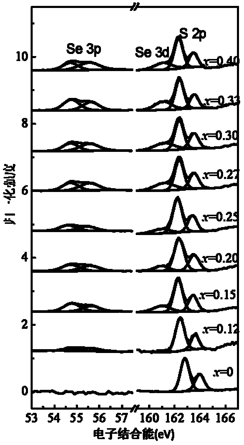
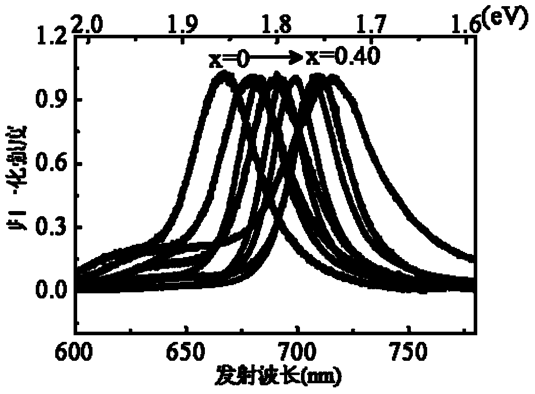
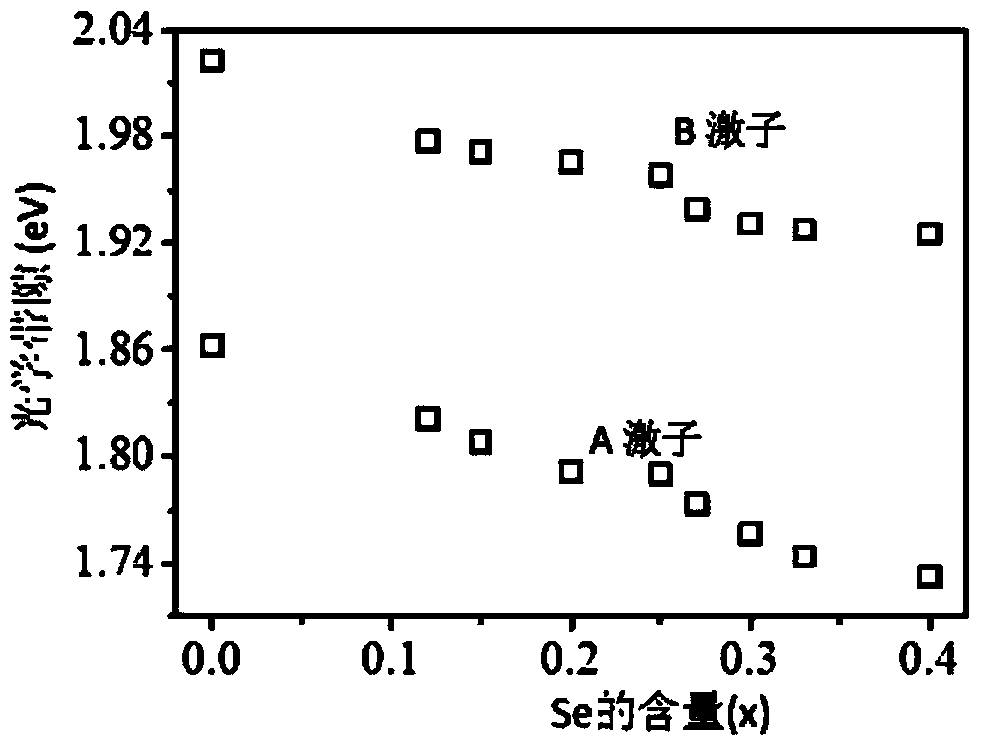
[0086] The heating volatilization temperature of molybdenum sulfide and molybdenum selenide in step (4), because the volatilization temperature of molybdenum sulfide and molybdenum selenide is different, the volatilization amount of the two is different, and the obtained two-dimensional semiconductor alloy MoS 2(1-x) Se 2x The growth results of are also different, specifically as described in Table 1;

[0087] Table 1 MoS obtained at different volatilization temperatures 2(1-x) Se 2x growth results

[0088] serial number T 硒化钼 (℃) T 硫化钼 (℃) ΔT (°C) x value Optical bandgap (eV) Emission wavelength (nm) 1 —— 940 —— 0 1.862±0.004 665~670nm 2 940 940 0 0.12 1.820±0.007 678~683 3 945 940 5 0.15 1.808...

Embodiment 3

[0098] A method for preparing a two-dimensional semiconductor alloy using a chemical vapor deposition device, the chemical vapor deposition device is the same as in Example 1, and the difference between the method and Example 1 is:

[0099] The silicon substrate in step (1) directly adopts commercially purchased silicon wafers (high P-silicon wafers purchased from Hefei Kejing Technology Co., Ltd., resistance value 0.02-0.6Ω, 0.5mm×4 inches), and cuts to obtain 6×8mm The flakes were obtained after ultrasonic treatment of acetone, ethanol, and ultrapure water three times each;

[0100] Step (3) The step of removing the oxidizing gas is: evacuate the inside of the quartz tube to 1-2Pa, pass in argon gas, and then evacuate to 1-2Pa again, repeat 3 times;

[0101] The flow rate of the protective gas introduced in step (4) is 10 sccm; the heating temperatures of molybdenum sulfide and molybdenum selenide in the quartz tube are 940°C and 990°C respectively; the mass ratio of molybde...


PUM


Abstract

The invention relates to a method for preparing a two-dimensional semiconductor alloy. The general formula of the two-dimensional semiconductor alloy is MoS2(1-x)Se2x, wherein x is more than 0 and less than or equal to 1. The method comprises: heating molybdenum sulfide and molybdenum selenide placed in quartz tubes respectively in an oxygen-free environment till volatilizing, keeping a volatilization temperature, and performing chemical vapor deposition on the volatilized molybdenum sulfide and molybdenum selenide on a silicon substrate under the action of introduced protective gas flow to form the two-dimensional semiconductor alloy material. The provided two-dimensional semiconductor alloy MoS2(1-x)Se2x can realize continuous adjustment of band gaps by adjusting the value of xl and the band gap adjustment of the two-dimensional semiconductor alloy MoS2(1-x)Se2x is realized by controlling the volatilization quantity of the molybdenum sulfide and the molybdenum selenide.

Description

technical field [0001] The invention belongs to the field of two-dimensional semiconductor alloys, in particular to a single-layer two-dimensional semiconductor alloy with continuously adjustable band gap, its preparation method and application. Background technique [0002] Two-dimensional semiconductor nanofilms with atomic thickness, such as transition metal chalcogenides, have a certain band gap and high on-off ratio, and have great application prospects in nanoelectronic devices. However, practical applications require two-dimensional nanoscale thin-film semiconductor materials with more band gaps to meet the needs of nanoelectronic devices in various environments. And the single-layer two-dimensional atomic crystal with adjustable continuous bandgap plays an important role in promoting the fields of full-spectrum detection and photoelectric conversion. [0003] Chalcogenides of transition metals (S and Se), MoS 2 、WS 2 、MoSe 2 It has a graphene-like structure, whic...

Claims


Application Information

Patent Timeline
IPC IPC(8): C23C16/06C23C16/448
Inventor 谢黎明冯晴亮张锦
Owner THE NAT CENT FOR NANOSCI & TECH NCNST OF CHINA
Why Eureka
Try Eureka