Ion sensitive field effect transistor and preparation process thereof

A field-effect transistor, ion-sensitive technology, applied in measurement devices, material analysis by electromagnetic means, instruments, etc., can solve the problems of reducing the accuracy and sensitivity of measuring ion concentration, reducing the signal-to-noise ratio of devices, etc.

Inactive Publication Date: 2014-07-23
FUDAN UNIV
View PDF9 Cites 1 Cited by
  • Summary
  • Abstract
  • Description
  • Claims
  • Application Information

AI Technical Summary

Problems solved by technology

[0004] From the above description of the working principle of the ion-sensitive field effect transistor in the prior art, it can be known that the generated source-drain current flows from the source electrode 102 to the drain electrode 103 through the contact interface between the gate insulating layer 104' and the semiconductor substrate 101. It can be seen from the preparation process of ion-sensitive field effect transistors in the prior art that the gate insulating layer 104' is generally made of silicon dioxide, and the semiconductor substrate 101 is generally made of silicon material, and the contact interface between the gate insulating layer 104 and the semiconductor substrate 101 must be There will be surface defects and surface roughness. Carriers flow through such a contact interface and are scattered by the contact interface. The entire device will inevitably generate measurement current noise due to surface defects and surface roughness during measurement, thus reducing The signal-to-noise ratio of the entire device, which in turn reduces the accuracy and sensitivity of the measured ion concentration of the entire device

Method used


Image

  • Ion sensitive field effect transistor and preparation process thereof
  • Ion sensitive field effect transistor and preparation process thereof
  • Ion sensitive field effect transistor and preparation process thereof

Examples


Embodiment approach

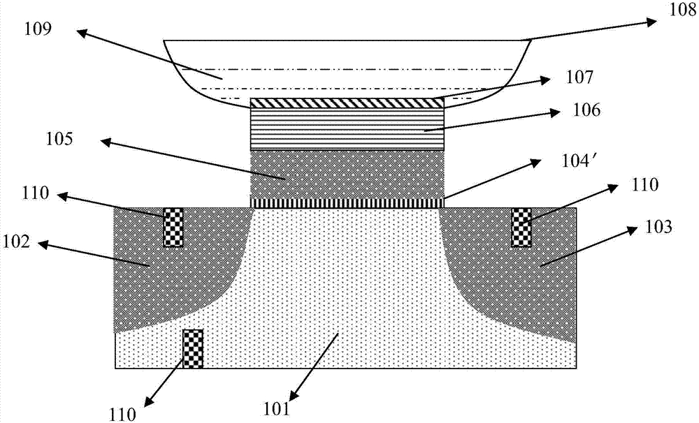
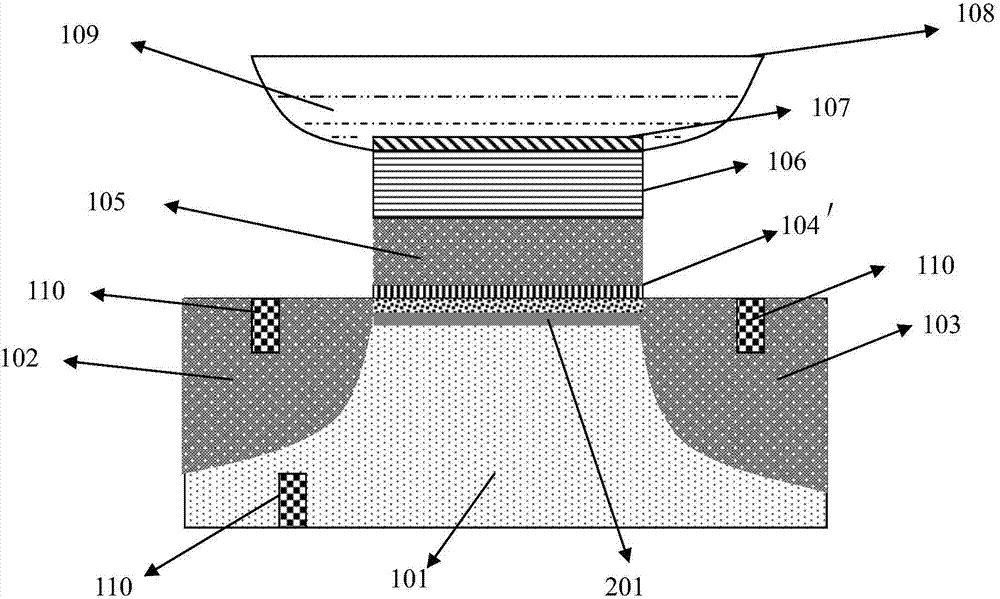
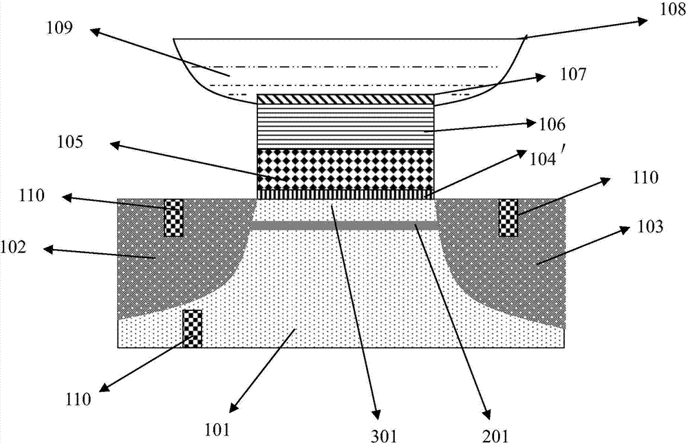
[0075] In this embodiment, since the conduction band positions of the energy bands of Si and SiGe are relatively close, and the forbidden band width of the SiGe material is smaller than that of the silicon material, holes can be gathered in the valence band region. When a current is formed between the source 102 and the drain 103 , holes tend to pass through the SiGe material with a lower forbidden band width rather than through the substrate extension layer 301 made of silicon. Compared with the first embodiment, there is no dopant ion of the same doping type as the buried channel in the substrate extension layer 301 in this embodiment, and the holes tend to all come from the SiGe buried channel with a smaller forbidden band width. 201 passes, and the mobility of holes in SiGe is greater than that in Si material, so that the current density will increase, and the sensitivity and accuracy of the current measurement of the entire device will be improved.

[0076] This embodimen...


PUM

PropertyMeasurementUnit
thicknessaaaaaaaaaa

Abstract

Relating to transistors, the invention discloses an ion sensitive field effect transistor and a preparation process thereof. The ion sensitive field effect transistor comprises a semiconductor substrate, a gate insulating layer, a source electrode and a drain electrode formed by doping, and a buried channel with the same doping type to the source electrode and the drain electrode. The buried channel is in the semiconductor substrate and near the upper surface, and the buried channel and the upper surface of the semiconductor substrate do not contact. The source electrode and the drain electrode are respectively located on two sides of the buried channel. The gate insulating layer is positioned on the semiconductor substrate above the buried channel. Compared with the prior art, when current is generated between the source electrode and the drain electrode in the transistor provided by the invention, the current flows through the buried channel in priority rather than pass through a contact interface between the gate insulating layer and the semiconductor substrate, thereby avoiding current measurement noise generated by surface defects of the contact interface, and preventing surface carrier scattering from reducing the signal-to-noise ratio and ion measurement sensitivity of the device.

Description

technical field [0001] The invention relates to a transistor, in particular to an ion sensitive field effect transistor and a preparation process thereof. Background technique [0002] In the prior art, the structure of the ion sensitive field effect transistor ISFET device is as follows figure 1 shown. Including a semiconductor substrate 101, a gate insulating layer 104' located in a predetermined area on the semiconductor substrate, a source electrode 102 and a drain electrode 103 formed by doping in the semiconductor substrate 101 located on both sides of the upper insulating layer 104, located on the gate insulating layer 104 The gate 105 formed by doping on the layer, the metal compound layer 106 on the gate 105, the ion sensitive film 107 on the metal compound layer 106 and the source 102, the drain 103 and the semiconductor substrate 101 on the backside metal silicide contact region 110 . [0003] The tested solution 109 is injected into the solution tank 108, and ...

Claims


Application Information

Patent Timeline
Patent Type & Authority Applications(China)
IPC IPC(8): G01N27/414
Inventor 吴东平曾瑞雪文宸宇张世理
Owner FUDAN UNIV
Why Eureka
Try Eureka