A kind of van der Waals dielectric material and its preparation method and application

A technology of dielectric materials and field effect transistors, applied in the field of two-dimensional material preparation, to achieve the effects of film thickness, good insulation properties, and good device properties

Active Publication Date: 2022-01-25
HUAZHONG UNIV OF SCI & TECH
View PDF0 Cites 0 Cited by
  • Summary
  • Abstract
  • Description
  • Claims
  • Application Information

AI Technical Summary

Problems solved by technology

The integration of such devices relies on fixed-point transfer technology, and there are still many technical difficulties in the large-scale preparation of such devices.

Method used


Image

  • A kind of van der Waals dielectric material and its preparation method and application
  • A kind of van der Waals dielectric material and its preparation method and application
  • A kind of van der Waals dielectric material and its preparation method and application

Examples


preparation example Construction

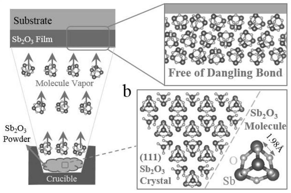
[0033] A method for preparing a van der Waals dielectric material provided by an embodiment of the present invention, such as figure 1 shown, including the following steps:

[0034] Inorganic molecular crystals are used as the evaporation source, and the method of thermal evaporation is adopted. Due to the weak van der Waals interaction between molecules, the evaporation source can be sublimated at a relatively low temperature under high vacuum conditions, so the internal structure of the molecule can be destroyed. In the case of high vacuum, the inorganic molecular crystals are sublimated to form molecular vapor, and then evaporated to obtain a van der Waals film. Since there are no unsaturated chemical bonds in the inorganic molecules, the surface of the prepared van der Waals film has no dangling bonds, and the van der Waals dielectric material is completed. preparation.

[0035] Further, the molecular crystal Sb with a band gap of 4eV 2 o 3 The powder is used as an evap...

Embodiment 1

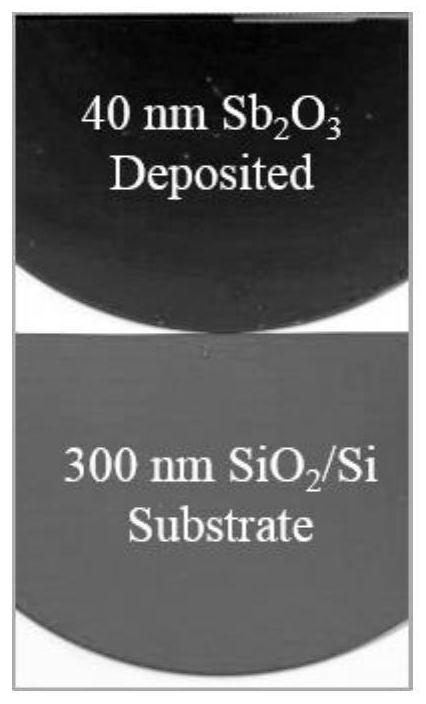
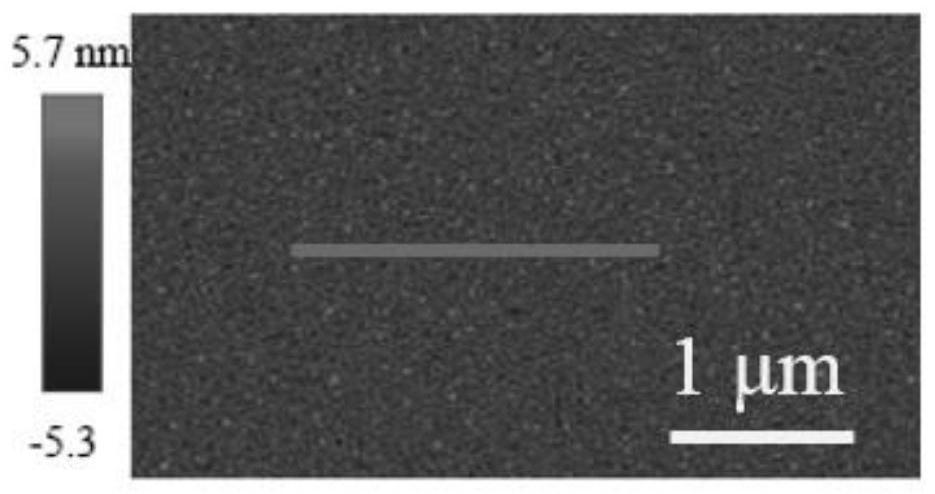
[0041] Choose inorganic molecular crystal Sb 2 o 3 As the evaporation source, silicon oxide is selected as the substrate, the molecular structure is maintained during the evaporation process, and the Sb evaporated on the substrate 2 o 3 There are no dangling bonds on the surface of the film, resulting in Sb 2 o 3 substrate. Such as figure 2 As shown, it is Sb with a thickness of 40nm prepared on a silicon oxide substrate 2 o 3 Thin film and substrate before evaporation, it can be seen that Sb on the entire substrate 2 o 3 The film has high uniformity; as Figure 3a and Figure 3b Shown, is the Sb under the atomic force microscope 2 o 3 The substrate and its surface relief curve, it can be seen that the Sb 2 o 3 The film is smooth and free of defects such as voids; Figure 4 Shown, for Sb 2 o 3 Raman optical characterization of the film, the results show that its Raman spectrum is consistent with that of the evaporated Sb 2 o 3 The Raman spectra of the powde...

Embodiment 2

[0043] Choose inorganic molecular crystal Sb 2 o 3 As the evaporation source, transparent glass is selected as the substrate, and the Sb evaporated on the substrate 2 o 3 No dangling bonds on film surface; test for Sb 2 o 3 The absorption spectrum of the thin film, such as Figure 5 As shown, by measuring the absorption spectrum, its forbidden band width is determined to be 4.0eV, indicating that Sb 2 o 3 Thin films are insulators.


PUM


Abstract

The invention belongs to the field of two-dimensional material preparation, and specifically discloses a van der Waals dielectric material and its preparation method and application. Sublimation occurs under high vacuum while maintaining its complete molecular structure, so that the van der Waals film is obtained by evaporation. Since there is no unsaturated chemical bond in the inorganic molecule, there is no dangling bond on the surface of the van der Waals thin film, thereby completing the preparation of the van der Waals dielectric material. The van der Waals thin film prepared by the present invention can be used as a dielectric material for two-dimensional material electronic devices, and can significantly reduce the carrier scattering source in the two-dimensional channel material, thereby ensuring that the two-dimensional material has high mobility; at the same time, the preparation process and The semiconductor preparation process is compatible, and it is easy to realize large-scale preparation and integration.

Description

technical field [0001] The invention belongs to the field of two-dimensional material preparation, and more specifically relates to a van der Waals dielectric material and its preparation method and application. Background technique [0002] Since the discovery of graphene, two-dimensional semiconductor materials have aroused extensive research interests due to their great application prospects in next-generation transistors. This is mainly due to the fact that it can still maintain high carrier mobility under the condition of atomic-level thickness, which can effectively avoid the short channel effect and other problems that current silicon-based transistors face when they are further miniaturized. However, when two-dimensional materials are integrated into devices, their physical properties (including mobility, which determines important parameters such as transistor switching speed) are easily affected by their surrounding environment. In SiO 2 The mobility of two-dimen...

Claims


Application Information

Patent Timeline
Patent Type & Authority Patents(China)
IPC IPC(8): C23C14/08C23C14/24H01L29/51H01L29/778
CPCC23C14/08C23C14/24H01L29/517H01L29/778
Inventor 翟天佑刘开朗金宝李会巧
Owner HUAZHONG UNIV OF SCI & TECH
Why Eureka
Try Eureka