A nickel-doped copper oxide thin film transistor and a preparation method thereof

A thin-film transistor and copper oxide technology, which is applied in the direction of transistors, semiconductor/solid-state device manufacturing, semiconductor devices, etc., can solve problems such as difficult preparation of p-type metal oxide thin films, and achieve less hole scattering and high hole transport capacity , The effect of improving the quality of the contact interface

Active Publication Date: 2018-12-18
EAST CHINA NORMAL UNIV
View PDF6 Cites 0 Cited by
  • Summary
  • Abstract
  • Description
  • Claims
  • Application Information

AI Technical Summary

Problems solved by technology

However, the parameters such as the mobility of p-type metal oxide thin film transistors using holes as carriers are still relatively low compared to n-type metal oxide transistors using electrons as carriers.
Affected by material stability and process complexity, it is still difficult to prepare high-quality p-type metal oxide thin films

Method used


Image

  • A nickel-doped copper oxide thin film transistor and a preparation method thereof
  • A nickel-doped copper oxide thin film transistor and a preparation method thereof
  • A nickel-doped copper oxide thin film transistor and a preparation method thereof

Examples


Embodiment

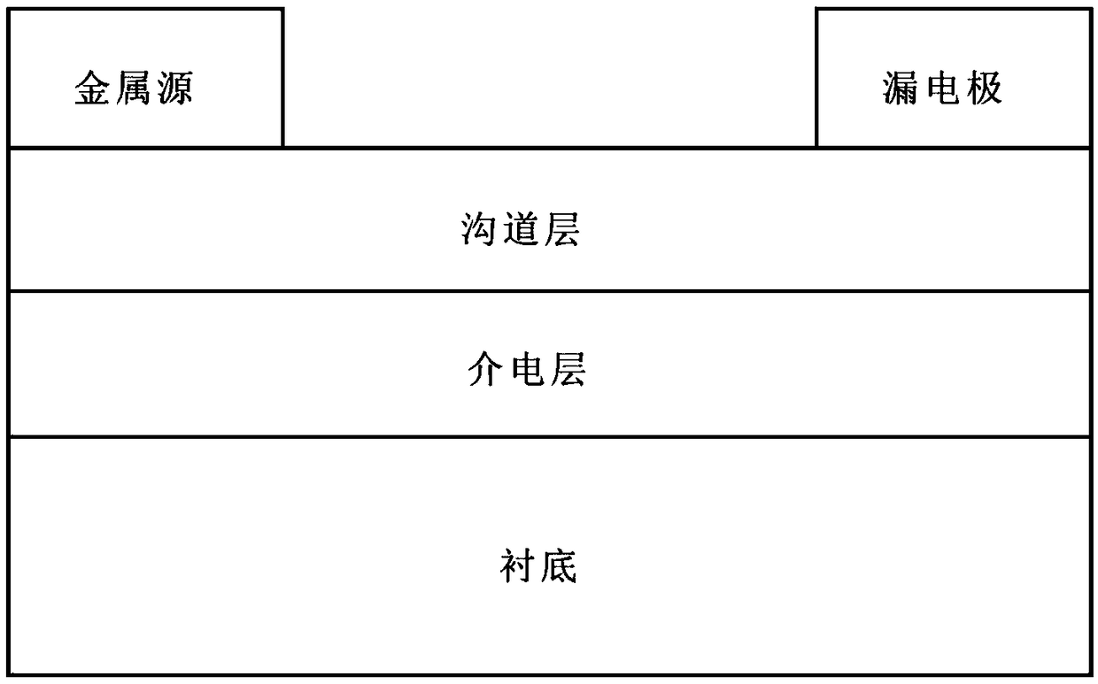
[0022] refer to figure 1 , a kind of preparation method of nickel-doped copper oxide thin film transistor, it comprises the steps:

[0023] 1.1. Preparation of precursor solution for nickel-doped copper oxide film

[0024] Select glycerol and deionized water, prepare a mixed solution at a volume ratio of 1:1-4, then take nickel nitrate and copper nitrate and dissolve them in the mixed solution at a molar ratio of 1-5:999-95, and configure 0.1 mol / L concentration of the precursor solution, stirred by magnetic force for 6-12 hours; to obtain the precursor solution of the nickel-doped copper oxide film;

[0025] 1.2. Preparation of nickel-doped copper oxide film

[0026] Select a heavily doped silicon wafer as the substrate, wash it with acetone: time, 20 minutes; wash with deionized water: time, 20 minutes; wash with ethanol: time, 20 minutes; place in an annealing furnace for annealing treatment: preheat Time, 20 minutes, preheating temperature, 600 ℃;

[0027] Spin-coat th...


PUM

PropertyMeasurementUnit
thicknessaaaaaaaaaa
thicknessaaaaaaaaaa
thicknessaaaaaaaaaa

Abstract

A nickel-doped copper oxide thin film transistor and a preparation method thereof are disclosed. A precursor solution is prepared, the precursor solution is spin-coated on a heavily doped silicon wafer to form a nickel-doped copper oxide film, a metal source and a drain electrode are prepared on the nickel-doped copper oxide film by using a mask plate, and the preparation of a back gate structuretransistor, i. e., a p-type thin film transistor, is completed. The performance of the back gate structure transistor is obviously improved compared with that of the copper oxide thin film transistor.The nickel-doped copper oxide thin film prepared by the invention has the beneficial effects of high quality of the thin film, reduced carrier scattering, high hole transmission capability and low hole scattering, so that the quality of the contact interface between the thin film and the dielectric layer and the electrode is improved, and the purpose of improving the mobility of the thin film transistor is achieved.

Description

technical field [0001] The invention relates to the technical field of preparing thin film transistors by a solution method, in particular to a method for preparing a nickel-doped copper oxide thin film transistor. Background technique [0002] Thin Film Transistor (TFT) is the core device of flat panel display, and each pixel depends on TFT for switching and driving. According to the different semiconductor materials of the TFT active layer, the current mainstream TFT technology is divided into hydrogenated amorphous silicon TFT, low temperature polysilicon TFT and amorphous oxide TFT. Among them, oxide TFT is considered to be the most likely to be used in the next generation of flat panel displays due to its advantages such as high mobility, good large-area uniformity, and low manufacturing process temperature. [0003] On the other hand, the CMOS structure is an important circuit structure in integrated circuits. The CMOS structure is a complementary device structure com...

Claims


Application Information

Patent Timeline
Patent Type & Authority Applications(China)
IPC IPC(8): H01L21/02H01L29/786H01L21/336
CPCH01L21/02381H01L21/02565H01L21/02584H01L21/02628H01L29/66969H01L29/7869
Inventor 李文武杨宇杨佳燕胡志高褚君浩
Owner EAST CHINA NORMAL UNIV
Why Eureka
Try Eureka