A transfer transistor structure

A transfer transistor and reset tube technology, which is applied in the manufacture of semiconductor/solid-state devices, electrical components, circuits, etc., can solve the problems of weakening the output signal at the signal output end, high power consumption, and increasing the difficulty of turning on, so as to reduce the loss of voltage drop, Improve the output intensity, power consumption has no effect

Active Publication Date: 2016-09-07
SHANGHAI HUALI MICROELECTRONICS CORP
View PDF6 Cites 0 Cited by
  • Summary
  • Abstract
  • Description
  • Claims
  • Application Information

AI Technical Summary

Problems solved by technology

[0008] 1) The turn-on voltage of the transfer transistor is increased, which increases the difficulty of turning it on, resulting in a delay in signal transmission of the CMOS image sensor;
[0009] 2) The increase in the length of the conductive channel increases the volume of the CMOS image sensor chip, which consumes a lot of power during use, and does not conform to the development trend of miniaturization and intensive integration of semiconductor devices;
[0011] 4) Although the current method is beneficial to increase the inversion region, there is still the problem of a rapid decrease in the electron input rate of the photodiode, which in turn leads to the problem that the output signal at the signal output terminal is significantly weakened

Method used


Image

  • A transfer transistor structure
  • A transfer transistor structure
  • A transfer transistor structure

Examples


Embodiment

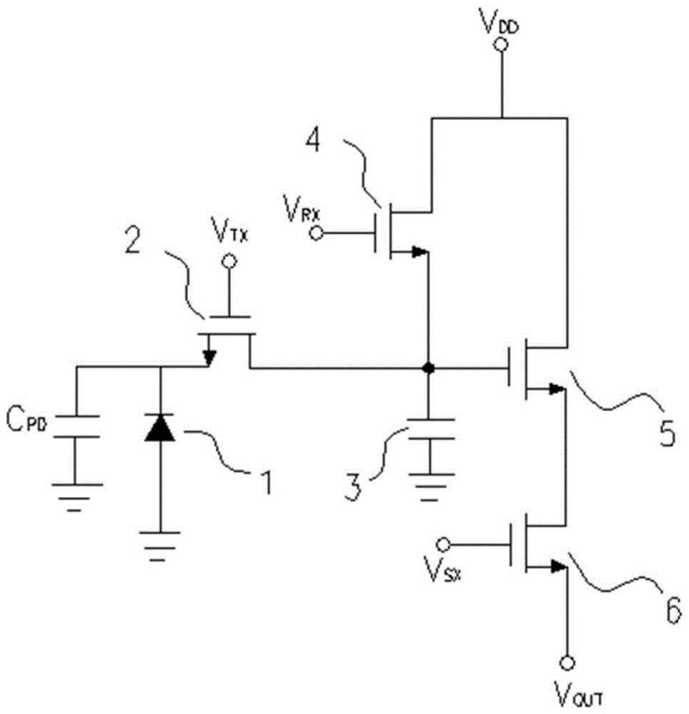
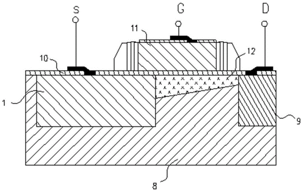
[0034] Such as Figure 4 As shown, a transmission transistor structure for enhancing the output signal of a CMOS image sensor includes a photodiode 1, a P-type silicon base 8, a drain terminal 9, an insulating layer 10, and a polysilicon gate 11; the photodiode 1 serves as the source terminal of the transmission transistor 2, The source terminal and the drain terminal 9 form an NPN junction on the P-type silicon base 8. The photodiode 1, the P-type silicon base 8, the drain terminal 9, the insulating layer 10 and the polysilicon gate 11 are used in the CMOS image sensor. The CMOS image sensor also includes Amplifier 5, reset tube 4, capacitor 3, strobe 6, V TX Power supply, V RX Power supply, V DD Power and V SX The drain terminal 9 of the transfer transistor 2 is connected to the gate of the amplifier 5 and the source of the reset tube 4, and the crystalline silicon gate of the transfer transistor 2 is connected to the power source V TX Connected; the photodiode 1 of the t...


PUM


Abstract

A transmission transistor structure capable of enhancing signals output by a CMOS image sensor comprises a photodiode, a P-type silicon substrate, a drain terminal, an insulating layer, a polycrystalline silicon grid, a conductive channel and a heavily-doped region. The photodiode of a transmission transistor serves as a single photo-electric conversion diode and is responsible for converting optical signals to electric signals, and meanwhile, the photodiode of the transmission transistor also serves as the source end of the transmission transition responsible for electron transmission in the structure of the CMOS image sensor and is directly connected with the transmission transistor. The heavily-doped region with the junction depth being 0.12-0.18 micrometer is formed at the position, close to the polycrystalline silicon grid of the transmission transistor, of the photo diode through ion implantation, and the injected doping ion concentration is higher than the originally-injected doping ion concentration of the photodiode. According to the transmission transistor structure, when the CMOS image sensor outputs signals, the phenomenon that the conductive channel is pinched off too early can be avoided, photoelectrons are transmitted out as many as possible, and therefore the output strength of electric signals of the CMOS image sensor is enhanced.

Description

Technical field [0001] The present invention relates to the technical field of integrated circuit manufacturing, in particular to a transmission transistor structure in a CMOS (Complementary Metal Oxide Semiconductor) image sensor chip manufacturing process. Background technique [0002] In the basic structure of CMOS image sensor chips, transfer transistors are generally used, such as figure 1 , figure 2 with image 3 As shown, 1 is a photodiode, 2 is a transfer transistor, 3 is a capacitor, 4 is a reset tube, 5 is an amplifier, 6 is a gate, 7 is polysilicon, 8 is a P-type silicon base, and 9 is a drain terminal. 10 is an insulating layer, 11 is a polysilicon gate, and 12 is a conductive channel; each CMOS image sensor generates a pixel, and each pixel contains a photodiode and a transmission transistor. The function of the transmission transistor is to increase the sensitivity of the circuit. The photodiode 1 is converted into photoelectrons, which enter the circuit through th...

Claims


Application Information

Patent Timeline
Patent Type & Authority Patents(China)
IPC IPC(8): H01L27/146H01L21/265
Inventor 杜文慧杨荣华王艳生
Owner SHANGHAI HUALI MICROELECTRONICS CORP
Why Eureka
Try Eureka