Reflection cavity mirror structure for high-speed Q modulation and wavelength tunable type waveguide laser

A laser and tuning wave technology, applied in the field of reflective cavity mirror structure, can solve the problems of complex fabrication, inability to increase the modulation bandwidth, and inability to achieve, and achieve the effect of simple process

Inactive Publication Date: 2014-07-23
ZHEJIANG UNIV
View PDF4 Cites 14 Cited by
  • Summary
  • Abstract
  • Description
  • Claims
  • Application Information

AI Technical Summary

Problems solved by technology

However, the problem is that the modulation bandwidth cannot be improved due to the limitation of laser relaxation oscillation.
In integrated optics technology, high-efficiency optical path reflection is achieved. Simple end-face reflection requires the production of

Method used


Image

  • Reflection cavity mirror structure for high-speed Q modulation and wavelength tunable type waveguide laser
  • Reflection cavity mirror structure for high-speed Q modulation and wavelength tunable type waveguide laser
  • Reflection cavity mirror structure for high-speed Q modulation and wavelength tunable type waveguide laser

Examples


Embodiment 1

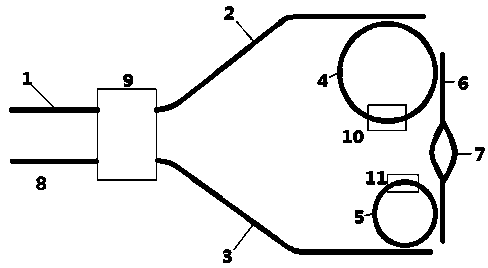
[0023] Such as figure 2 As shown, the device is made of silicon-on-insulator (SOI) material, the thickness of the top silicon layer is 220 nm, and the thickness of the silicon dioxide buried layer is 1 μm. Using CMOS technology, through deep ultraviolet lithography and silicon dry etching, a ridge-shaped optical waveguide with a width of 400nm and a depth of 180nm is produced. After the silicon dry etching is completed, the chemical vapor deposition method is used to cover 2μm Silicon layer, composed of figure 2 The basic device structure shown.

[0024] A symmetrical Y branch structure 19 is used in the device as a beam splitting coupling structure. The two optical microrings in the device have radii of 5 μm and 7 μm, respectively. The gap between the optical microring and the two parallel waveguides is 180 nm. The tuning of the optical microring utilizes the thermo-optic effect of silicon to fabricate a heating electrode corresponding to the microring on the silicon di...

Embodiment 2

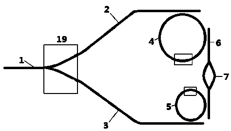
[0027] Such as image 3 As shown, the device is made of silicon-on-insulator (SOI) material, the thickness of the top silicon layer is 220 nm, and the thickness of the silicon dioxide buried layer is 1 μm. Using CMOS technology, through deep ultraviolet lithography and silicon dry etching, a ridge-shaped optical waveguide with a width of 400nm and a depth of 180nm is produced. After the silicon dry etching is completed, the chemical vapor deposition method is used to cover 2μm Silicon layer, composed of image 3 The basic device structure shown.

[0028] The X cross junction structure 29 is used as the beam splitting coupling structure in the device. The two optical microrings in the device have radii of 5 μm and 5 μm, respectively. The gap between the optical microring and the two parallel waveguides is 180 nm. The tuning of the optical microring utilizes the thermo-optic effect of silicon to fabricate a heating electrode corresponding to the microring on the silicon diox...

Embodiment 3

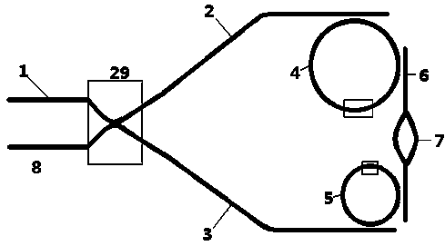
[0031] Such as Figure 4 As shown, the device is made of silicon-on-insulator (SOI) material, the thickness of the top silicon layer is 220 nm, and the thickness of the silicon dioxide buried layer is 1 μm. Using CMOS technology, through deep ultraviolet lithography and silicon dry etching, a ridge-shaped optical waveguide with a width of 400nm and a depth of 180nm is produced. After the silicon dry etching is completed, the chemical vapor deposition method is used to cover 2μm Silicon layer, composed of Figure 4 The basic device structure shown.

[0032] A directional coupler 39 is used as a beam splitting coupling structure in the device. The two optical microrings in the device have radii of 7 μm and 7 μm, respectively. The gap between the optical microring and the two parallel waveguides is 180 nm. The tuning of the optical microring utilizes the thermo-optic effect of silicon to fabricate a heating electrode corresponding to the microring on the silicon dioxide layer...


PUM

PropertyMeasurementUnit
Radiusaaaaaaaaaa

Abstract

The invention discloses a reflection cavity mirror structure for a high-speed Q modulation and wavelength tunable type waveguide laser. The reflection cavity mirror structure for the high-speed Q modulation and wavelength tunable type waveguide laser comprises a split beam coupling structure, a big tunable optical micro-ring, a small tunable optical micro-ring and a Mach-Zehnder modulation structure, wherein the split beam coupling structure serves as an input end and a reflection output end, the two optical micro-rings are connected with the split beam coupling structure by being coupled with a first waveguide evanescent wave and a second waveguide evanescent wave respectively so that wavelength tuning can be achieved, and the two ends of the Mach-Zehnder modulation structure are connected with corresponding optical micro-ring evanescent waves respectively in a coupled mode through straight waveguide, so that wavelength tuning of the laser is achieved. According to the reflection cavity mirror structure for the high-speed Q modulation and wavelength tunable type waveguide laser, the reflectivity can be adjusted rapidly, wavelength tuning can be achieved, and the reflection cavity mirror structure can be used for constructing the high-speed Q modulation and wavelength tunable type waveguide laser. Due to the adoption of the two optical micro-rings, the range of the adjustable wavelength of the environment can be widened according to the vernier and calipers effect.

Description

technical field [0001] The invention relates to an integrated optical device, in particular to a reflective cavity mirror structure for high-speed Q modulation and wavelength tunable waveguide lasers. Background technique [0002] High-speed optical modulation and wavelength division multiplexing are the main means to improve optical information transmission. The traditional direct modulation method is to directly control the driving current of the laser with the modulation signal to realize the information loading of the output optical signal. However, there is a problem that the modulation bandwidth cannot be increased due to the limitation of the relaxation oscillation of the laser. The indirect modulation method with an external modulator can greatly increase the modulation frequency, but because it processes the laser that has already been output from the laser, half of the energy in the external indirect modulation method is not used, which is very important for the e...

Claims


Application Information

Patent Timeline
IPC IPC(8): H01S5/10H01S5/06
Inventor 周志敏虞思城黄兆维杨龙志杨建义
Owner ZHEJIANG UNIV
Why Eureka
Try Eureka