Flat circuit board and manufacturing method thereof

A production method and flush line technology, applied in chemical/electrolytic methods to remove conductive materials, printed circuit components, printed circuit secondary treatment, etc., can solve the problem that circuit boards cannot meet the requirements of plane contact conduction and poor protection reliability and other problems, to achieve the effect of excellent flatness, high conductivity reliability, and improved reliability

Inactive Publication Date: 2014-07-23
邢台市海纳电子科技有限责任公司
View PDF3 Cites 26 Cited by
  • Summary
  • Abstract
  • Description
  • Claims
  • Application Information

AI Technical Summary

Problems solved by technology

[0003] One of the purposes of the present invention is to provide a flush circuit board to solve the problem that the traditional circuit board itself cannot meet the technical requirements of planar contact and conduction and has poor protection reliability

Method used


Image

  • Flat circuit board and manufacturing method thereof

Examples


Embodiment 1

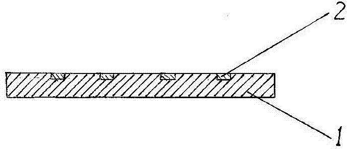
[0029] Such as figure 1 As shown, the flush circuit board of the present invention is provided with a conductive circuit pattern strip 2 on the insulating substrate 1, and the circuit pattern strip 2 is embedded in the upper surface of the insulating substrate 1, and the outer surface of the circuit pattern strip 2 is in contact with the The upper surfaces of the insulating substrate 1 are on the same plane.

[0030] The circuit graphic strip 2 is formed by thermally pressing the conductive copper foil layer bonded on the insulating substrate 1, after surface filming, circuit pattern transfer, etching and fading, and nickel-plating and gold-plating. embedded in the surface of the insulating substrate.

[0031] The circuit pattern strip 2 in the present invention is completely embedded in the interior of the insulating substrate 1, and the surface of the line has conductivity, which meets the requirements of surface contact and conduction. The biggest difference from the tradi...

Embodiment 2

[0033] The manufacturing method of flush circuit board of the present invention comprises the following steps:

[0034] 1. Material cutting: according to the product design requirements, use a cutting machine to cut the prepreg for circuit board production into the required size.

[0035] Precautions for prepreg preparation:

[0036] ①In a clean and dust-free environment, cut the roll material into strips, and then cut them into individual pieces with a paper cutter. The size is enlarged by 10mm according to the length and width of the single blank.

[0037] ②If there are defects such as broken fibers, large particles of jelly, and impurities on the prepreg, they should be removed. Clean spun gauze gloves should be worn during operation, and hand sweat and oil pollution are strictly prohibited.

[0038] ③ When cutting the prepreg, wear a mask to avoid inhaling resin powder. It is advisable to wear long shirts and trousers to avoid itching or allergies caused by resin po...


PUM


Abstract

The invention relates to a flat circuit board and a manufacturing process thereof. A conductive circuit graph strip is arranged on an insulation base board of the flat circuit board, the circuit graph strip is embedded in the upper surface of the insulation base board, and the outer surface of the circuit graph strip and the upper surface of the insulation base board are located on the same plane. The flat circuit board has the advantages of being high in reliability and good in smoothness. After the circuit graph strip is embedded in the insulation base board, circuit external damage is avoided, the strip is broken only when physical damage is caused to the base board, conductivity reliability is high, and the technical requirement for surface sliding contact communication is met. The flat circuit board is especially applicable to precision operation with the strict environment requirement in the fields of aerospace, aviation, military and medical treatment.

Description

technical field [0001] The invention relates to a printed circuit board, in particular to a flush circuit board and a manufacturing method thereof. Background technique [0002] The printed circuit board industry has been in my country for more than 40 years. With the acceleration of the upgrading of the electronic industry, the printed circuit board occupies an increasingly important position in the development of the national economy. Since my country replaced Japan as the world's largest printed circuit board manufacturing country in 2009, the printed circuit board industry has developed by leaps and bounds, playing an increasingly important role in all walks of life in the field of weak current. While the application field of printed circuit boards is expanding day by day, the incompatibility of traditional circuit boards in certain industries or in some special environments is also becoming more and more prominent. For example, traditional circuit boards lay circuits on...

Claims


Application Information

Patent Timeline
Patent Type & Authority Applications(China)
IPC IPC(8): H05K1/09H05K3/06H05K3/22
Inventor 张伯平
Owner 邢台市海纳电子科技有限责任公司
Why Eureka
Try Eureka