Preparation method of silicon nanowire array with excellent field emission performance and tip structure

A silicon nanowire array and field emission technology, applied in the field emission field, can solve the problems of staying, poor repeatability, etc., and achieve the effects of low cost, high yield, and improved monolayer property

Active Publication Date: 2014-07-30
TSINGHUA UNIV
View PDF9 Cites 6 Cited by
  • Summary
  • Abstract
  • Description
  • Claims
  • Application Information

AI Technical Summary

Problems solved by technology

At present, most silicon nanowire nanoelectronic devices are still in the laboratory research stage, their repeatability is poor, and there is still a considerable distance from the large-scale integration of nanodevices.

Method used


Image

  • Preparation method of silicon nanowire array with excellent field emission performance and tip structure
  • Preparation method of silicon nanowire array with excellent field emission performance and tip structure
  • Preparation method of silicon nanowire array with excellent field emission performance and tip structure

Examples


Embodiment 1

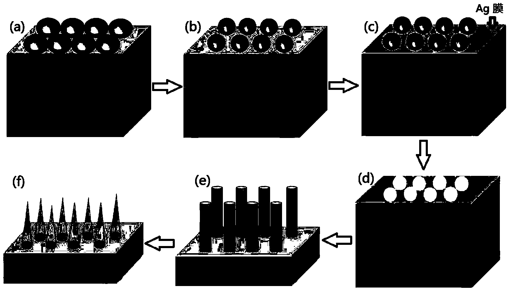
[0028] (1) The silicon substrate and the glass slide were ultrasonically cleaned with acetone, alcohol, and deionized water one by one and immersed in concentrated H 2 SO 4 and H 2 o 2 Hydrophilic treatment is carried out in a mixed solution with a volume ratio of 4:1;

[0029] (2) Arrange a single layer of close-packed PS beads on the silicon substrate, the method is as follows: dry the glass sheet and place it in the center of the watch glass, add deionized water to the watch glass until the water level is slightly higher than the glass sheet Surface: Slowly add the diluted aqueous solution of PS beads with a mass fraction of 0.5% and a diameter of 960 nm onto the glass sheet, the beads spread on the liquid surface, and stop the dripping after most of the liquid surface covers a single layer of beads; Drop 1mL of sodium dodecyl sulfate solution with a mass fraction of 1% from the edge of the watch glass, put the silicon chip into the watch glass, push it to the side where...

Embodiment 2

[0037] (1) The silicon substrate and the glass slide were ultrasonically cleaned with acetone, alcohol, and deionized water one by one and immersed in concentrated H 2 SO 4 and H 2 o 2 Hydrophilic treatment is carried out in a mixed solution with a volume ratio of 4:1;

[0038] (2) Arrange a single layer of close-packed PS spheres on the silicon substrate by self-assembly method. The method is as follows: dry the glass sheet and place it in the center of the watch glass, add deionized water to the watch glass to the water surface Slightly higher than the surface of the glass sheet; slowly drop the aqueous solution of PS beads with a mass fraction of 0.5% and a diameter of 980nm obtained by dilution onto the glass sheet, and the beads spread on the liquid surface until most of the liquid surface covers a single layer of beads Stop dripping; drop 1mL sodium dodecyl sulfate solution with a mass fraction of 1% from the edge of the watch glass, put the silicon chip into the watch ...

Embodiment 3

[0045] (1) The silicon substrate and the glass slide were ultrasonically cleaned with acetone, alcohol, and deionized water one by one and immersed in concentrated H 2 SO 4 and H 2 o 2 Hydrophilic treatment is carried out in a mixed solution with a volume ratio of 4:1;

[0046] (2) Arrange a layer of single-layer close-packed PS spheres on the silicon substrate by self-assembly method, the method is as follows: dry the glass sheet and place it in the center of the watch glass, add deionized water to the watch glass to the water surface Slightly higher than the surface of the glass sheet; slowly drop the aqueous solution of PS beads with a mass fraction of 0.5% and a diameter of 1000nm to the glass sheet, and the beads spread on the liquid surface until most of the liquid surface covers a single layer of beads Stop dripping; drop 1mL sodium dodecyl sulfate solution with a mass fraction of 1% from the edge of the watch glass, put the silicon chip into the watch glass, push it...


PUM

PropertyMeasurementUnit
current densityaaaaaaaaaa
lengthaaaaaaaaaa
diameteraaaaaaaaaa

Abstract

The invention discloses a preparation method of a silicon nanowire array with excellent field emission performance and a tip structure, and belongs to the technical field of field emission. The method comprises the following steps: firstly configuring single-layered PS (Polystyrene) spheres densely on a silicon substrate, carrying out reactive ion etching treatment on the PS spheres, adopting an electron beam evaporation method to plate silver, removing the PS spheres, carrying out silver catalytic corrosion to the substrate, and obtaining the silicon nanowire array with larger diameter; adopting a dry-method oxidation treatment to turn the silicon nanowires into the tip structure, further reducing the diameter of the silicon nanowires, and increasing the space between the silicon nanowires. The silicon nanowire array with the tip structure, prepared with the method, is of excellent field emission performance; the threshold voltage of the silicon nanowire array is 1.8 V per microns; the current stability is good; meanwhile, the single crystal performance of the silicon nanowires is good, so that the silicon nanowires can be regularly and densely configured in a large area, and the controllability of the draw ratio is strong. The method is low in cost, high in yield and good in controllability, so as to be applied to production of silicon-substrate field emission electronic devices.

Description

technical field [0001] The invention belongs to the technical field of field emission, in particular to a method for preparing a silicon nanowire array with excellent field emission performance and a tip structure. Background technique [0002] Silicon is the most important semiconductor in the field of electronic information technology; silicon and silicon oxides and nitrides are widely used in electrical interconnection integrated circuits due to their abundant content in the earth, low raw material prices, and mature preparation processes. Over the past half century, silicon-based microelectronics technology has been deeply developed and has become the core technology in the fields of computing, communication, automatic control and information processing. As an important class of one-dimensional semiconductor nanomaterials, silicon nanowires have good application prospects in nanodevices. At the same time, silicon nanowires have stable semiconductor properties and are co...

Claims


Application Information

Patent Timeline
Patent Type & Authority Applications(China)
IPC IPC(8): B82B3/00B82Y40/00
Inventor 吕沙沙李正操
Owner TSINGHUA UNIV
Why Eureka
Try Eureka