Miniature infrared gas detection sensor
A technology of gas detection and sensor
- Summary
- Abstract
- Description
- Claims
- Application Information
AI Technical Summary
Problems solved by technology
Method used
Image
Examples
Embodiment 1
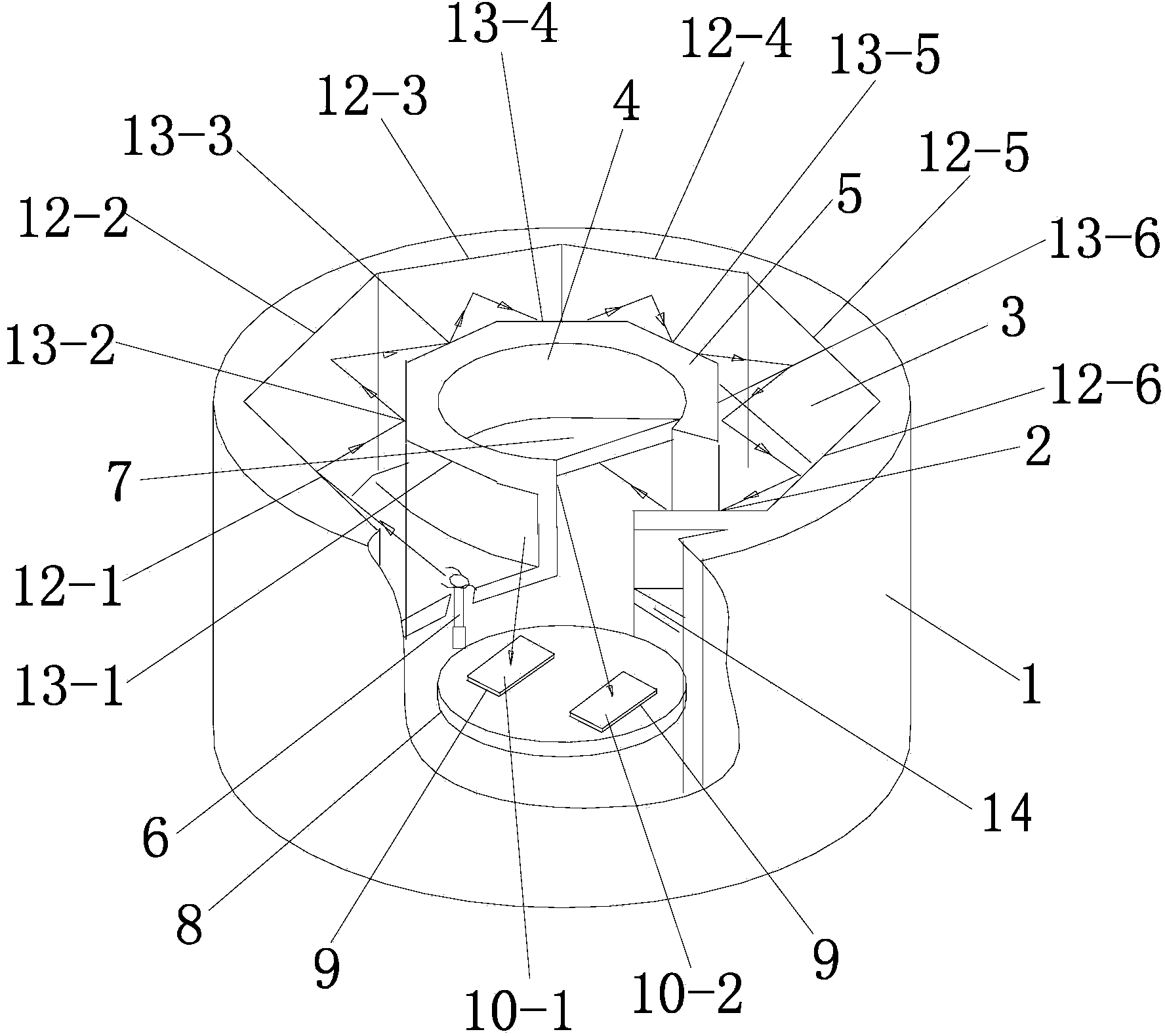
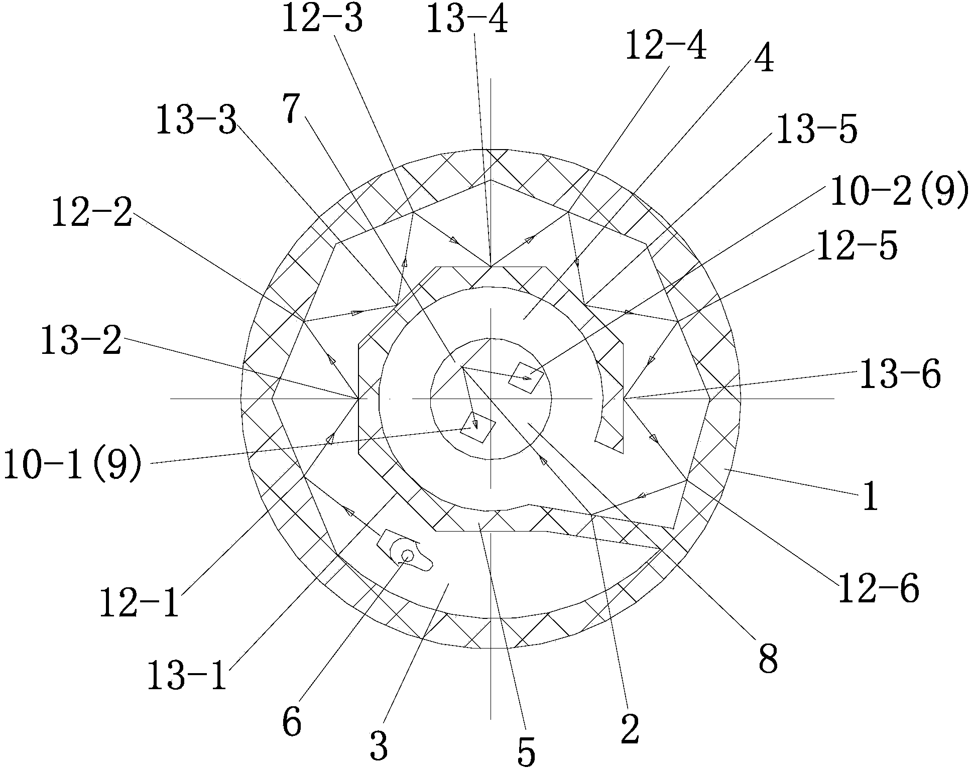
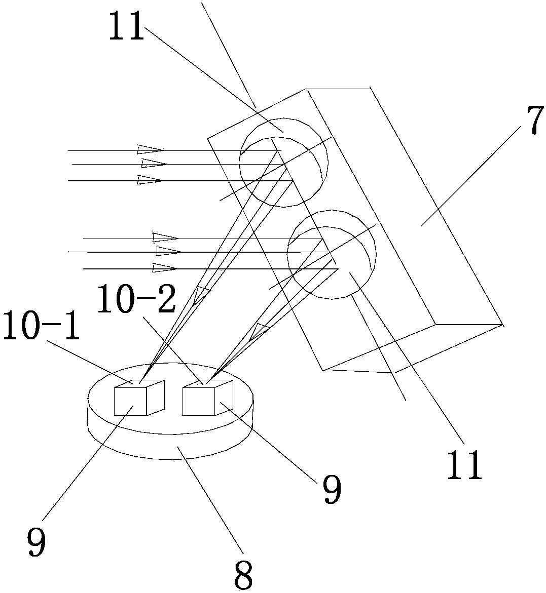
[0042] Such as figure 1 , figure 2 with image 3 As shown, the present invention includes a sensor housing 1 and an air chamber partition plate 5 that is arranged inside the sensor housing 1 and divides the air chamber inside the sensor housing 1 into two parts, an outer air chamber 3 and an inner air chamber 4. The air chamber partition plate 5 is provided with an opening, and the side edge of the air chamber partition plate 5 on one side of the opening is connected to the sensor housing 1, and the middle and lower part of the external air chamber 3 is provided with a The chamber 3 is divided into upper and lower partitions 14. The outer air chamber 3 is located below the upper and lower partitions 14 and is provided with a light-emitting part that passes through the upper and lower partitions 14 and is used to emit infrared light. Infrared light source 6, the upper part of the inner air chamber 4 is obliquely provided with a slant plate 7, the bottom of the inner air cham...
Embodiment 2
[0051] The difference between this embodiment and Example 1 is: the preparation method of the solid solution lead selenide thin film is: step 1, lead powder, water, anhydrous sodium sulfate and selenium powder are according to the mass ratio of 1:3:6:1 Mix, then stir at 90°C for 20 hours at a constant temperature, and obtain a solid material after filtration; step 2, make the solid material described in step 1 into a film with a thickness of 1.75mm; step 3, place the film described in step 2 in In a nitriding furnace, the temperature is 780° C., and the temperature is constant for 10 hours under a mixed atmosphere of nitrogen and hydrogen to obtain a solid solution lead selenide film. All the other structures are the same as in Example 1.
Embodiment 3
[0053] The difference between this embodiment and Example 1 is: the preparation method of the solid solution lead selenide thin film is: step 1, lead powder, water, anhydrous sodium sulfate and selenium powder are according to the mass ratio of 1:3:6:1 Mix, then stir at 80°C for 25 hours at a constant temperature, and obtain a solid material after filtration; step 2, make the solid material described in step 1 into a film with a thickness of 2 mm; step 3, place the film described in step 2 in a osmotic In a nitrogen furnace, at a temperature of 860° C. and a mixed atmosphere of nitrogen and hydrogen, a constant temperature treatment was carried out for 8 hours to obtain a solid solution lead selenide thin film.
[0054] The working process of the present invention is: the infrared light emitted by the mid-infrared light source 6 is first irradiated in parallel on the first outer reflective mirror 12-1 in the outer air chamber 3, and then irradiated into the second middle after ...
PUM
| Property | Measurement | Unit |
|---|---|---|
| thickness | aaaaa | aaaaa |
| wavelength | aaaaa | aaaaa |
| diameter | aaaaa | aaaaa |
Abstract
Description
Claims
Application Information


