Transmission electron microscope film window for in-situ high-resolution observation of electric field induced phase transition process of phase transition material

A phase change material and transmission electron microscope technology, applied in the field of transmission electron microscope film windows and transmission electron microscope film windows, can solve the problem that phase change materials cannot be directly observed, and achieve the effects of high-resolution observation, avoidance of damage, and high success rate.

Inactive Publication Date: 2014-07-30
BEIJING UNIV OF TECH
View PDF5 Cites 5 Cited by
  • Summary
  • Abstract
  • Description
  • Claims
  • Application Information

AI Technical Summary

Problems solved by technology

[0004] The purpose of the present invention is to overcome the defect that the phase change material in the vertical phase change memory used in practical applications is in the middle of the device and cannot be directly observed, and to provide a transmission electron micr...

Method used


Image

  • Transmission electron microscope film window for in-situ high-resolution observation of electric field induced phase transition process of phase transition material
  • Transmission electron microscope film window for in-situ high-resolution observation of electric field induced phase transition process of phase transition material
  • Transmission electron microscope film window for in-situ high-resolution observation of electric field induced phase transition process of phase transition material

Examples


Embodiment 1

[0036] The preparation method of the transmission electron microscope for in-situ electrical test of the present invention comprises the following steps:

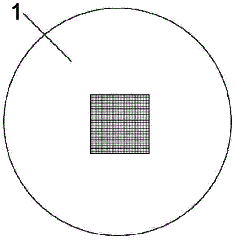
[0037] Step 1: Use an easy-to-process nickel sheet as a mask, and process the shape of the electrode on the mask. The hollow part is obtained by laser cutting or metal etching. The thickness of the mask is about 0.2mm, and the surface of the mask remains flat .

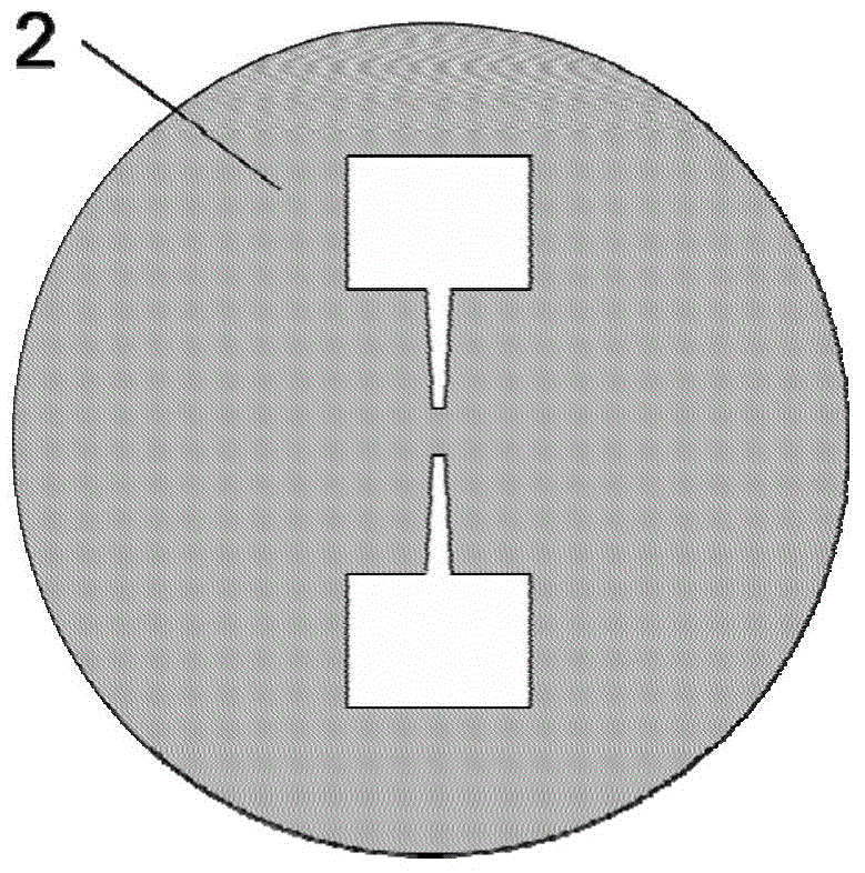
[0038] Step 2: Cover the mask on SiN x On the thin film window, a 200nm-thick Au is plated as an electrode by using a coating machine, and then the mask is removed to obtain an electrode, and the thin film material is between the electrodes. Due to the existence of the sputtering shadow area, the distance between the electrodes is designed to be 10 μm.

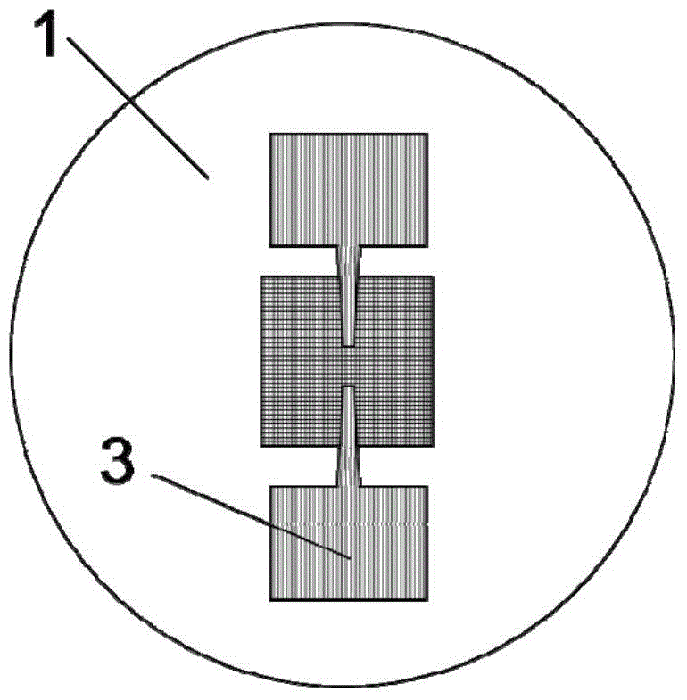
[0039] Step 3: FIB is used for electron beam deposition at both ends of the obtained electrodes to prepare Pt electrodes with a spacing of 1 μm. Then using a focused ion beam, the Si between the electrodes 3 N ...


PUM


Abstract

A transmission electron microscope film window for in-situ high-resolution observation of an electric field induced phase transition process of a phase transition material. The observation method comprises the following steps: processing electrode shapes on a metal sheet used as a mask plate by laser cutting or metal etching methods; covering a SiNx film window with the mask plate, plating metal electrodes by a film-plating machine; performing electron beam deposition at two ends of each obtained electrode by FIB to prepare Pt electrodes with small spacing; cutting and processing the SiNx film between the electrodes and the film between the Pt electrodes by focused ion beam to obtain a sample platform with a bridge structure; plating a film sample on the SiNx film window with the prepared electrodes by magnetron sputtering; connecting an electrified sample pole of a transmission electron microscope with the electrodes through a conductive adhesive, and performing in-situ electric experiments. The transmission electron microscope film window of the invention solves the problem that in-situ observation of the phase transition process of a phase transition material cannot be realized in a device, prevents sample damage caused by routine FIB preparation, and reduces the difficulty of sample preparation.

Description

technical field [0001] The invention relates to a thin-film window of a transmission electron microscope, and specifically uses a focused ion beam and a mask method to realize the preparation of a thin-film window for a transmission electron microscope that can observe the electrophase transition process of a phase-change material with high resolution in situ. It belongs to the field of in-situ testing of nanomaterial properties. Background technique [0002] The core of phase change memory (PCRAM) is a phase change material based on chalcogenides. At present, phase-change memory is considered to be the next-generation semiconductor storage technology that is most likely to replace the current mainstream product and become the mainstream product of future memory. Phase change storage is to use the huge difference in performance of phase change materials such as chalcogenides in the crystalline state and the amorphous state to realize 01 storage, such as the difference in op...

Claims


Application Information

Patent Timeline
IPC IPC(8): G01N23/04G01N1/28H01J37/26
Inventor 韩晓东邵瑞文郑坤张韬王疆靖张泽
Owner BEIJING UNIV OF TECH
Why Eureka
Try Eureka