Low-temperature polycrystalline silicon thin film transistor, manufacturing method thereof and display device

A thin-film transistor, low-temperature polysilicon technology, applied in transistors, semiconductor/solid-state device manufacturing, electrical solid-state devices, etc., can solve the problems of long diffusion distance, long time, long heat treatment time, etc., and achieve shortened distance and reduced time. , The effect of reducing process cost

Active Publication Date: 2014-08-13
BOE TECH GRP CO LTD
View PDF5 Cites 25 Cited by
  • Summary
  • Abstract
  • Description
  • Claims
  • Application Information

AI Technical Summary

Problems solved by technology

However, because the hydrogen in these methods usually needs to enter the active layer through the multi-layer film, the diffusion distance of hydrogen is very long. In order to fully carry out hydrogenation, it takes a long time to carry out heat treatment, which increases the process cost and time; at the same time, the long-term The heat treatment of time will cause a certain thermal impact on the TFT device, which will cause poor electrical properties of the TFT, especially when the size of the TFT is large, the impact is very large
[0005] The disadvantage of the existing technology is that hydrogen passes through more layers during the hydrogenation treatment, and the heat treatment time is longer, which leads to an increase in the process cost and easily leads to poor electrical performance of the thin film transistor.

Method used


Image

  • Low-temperature polycrystalline silicon thin film transistor, manufacturing method thereof and display device
  • Low-temperature polycrystalline silicon thin film transistor, manufacturing method thereof and display device
  • Low-temperature polycrystalline silicon thin film transistor, manufacturing method thereof and display device

Examples


Embodiment Construction

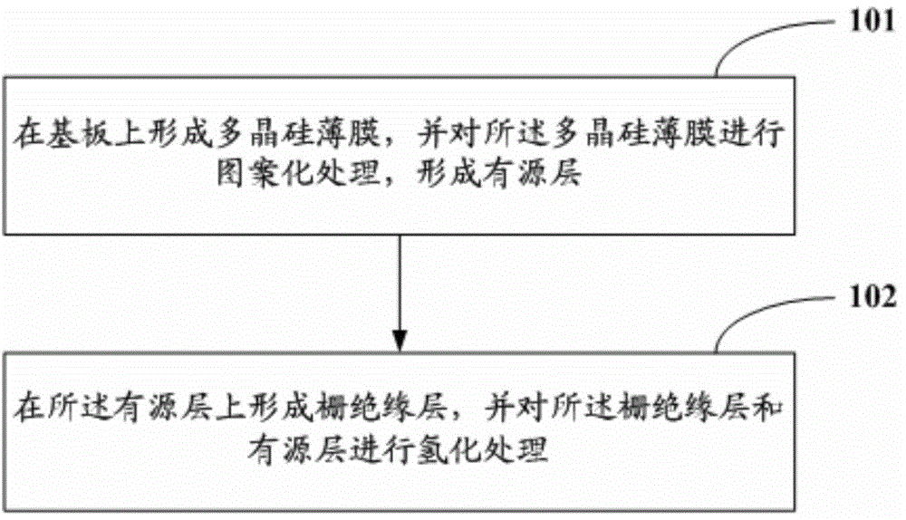
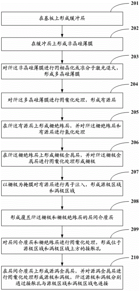
[0037] In order to solve the technical problem of long hydrogenation treatment time in the manufacturing process of the thin film transistor in the prior art, the present invention provides a low-temperature polysilicon thin film transistor, a manufacturing method thereof, and a display device. In this technical solution, after the gate insulating layer is fabricated, the gate insulating layer and the active layer are directly hydrogenated, and the hydrogen only needs to pass through the gate insulating layer to reach the interface between the gate insulating layer and the active layer to passivate the dangling bonds. and repair the grain boundary defects of the active layer, which greatly shortens the distance of hydrogen diffusion, reduces the time of the hydrogenation process, and thus greatly reduces the process cost of the thin film transistor. In order to make the purpose, technical solution and advantages of the present invention clearer, the following specific examples ...


PUM


Abstract

The invention relates to the technical field of display, and discloses a low-temperature polycrystalline silicon thin film transistor, a manufacturing method thereof and a display device. The manufacturing method of the low-temperature polycrystalline silicon thin film transistor comprises the steps that a polycrystalline silicon thin film is formed on a substrate, and is subjected to patterning processing to form an active layer; a grid insulating layer is formed on the active layer, and the grid insulating layer and the active layer are subjected to hydrogen treating. According to the technical scheme, after the grid insulating layer is manufactured, the grid insulating layer and the active layer are directly subjected to hydrogen treating, hydrogen just needs to penetrate through the grid insulating layer and reach an interface of the grid insulating layer and the active layer to carry out passivation on a dangling bond and overcome the crystal boundary defect of the active layer, hydrogen diffusion distance is greatly shortened, time of the hydrogenation process is reduced, and technical cost of the thin film transistor is greatly lowered.

Description

technical field [0001] The invention relates to the field of display technology, in particular to a low-temperature polysilicon thin film transistor, a manufacturing method thereof, and a display device. Background technique [0002] Low Temperature Poly-Silicon Thin Film Transistor (LTPS-TFT for short) has been widely used in displays due to its advantages of high mobility and stability, such as Active Matrix Organic Light-Emitting Display (Active Matrix Organic Light Emitting Diode (AMOLED for short), Active Matrix Liquid Crystal Display (AMLCD for short), etc. [0003] The preparation process of the TFT of the above-mentioned type of display is generally to form a polysilicon film on the substrate, and pattern the polysilicon film to form the active layer of the thin film transistor; form a gate insulating layer on the active layer; form a gate on the gate insulating layer; Then implant ions in the active layer to form the source region and the drain region respectively;...

Claims


Application Information

Patent Timeline
Patent Type & Authority Applications(China)
IPC IPC(8): H01L21/336H01L21/324H01L29/786
CPCH01L21/28158H01L27/1214H01L29/6675H01L29/78672H01L29/78618H01L21/3003H01L29/66757H01L29/78675H01L29/786H01L21/02274H01L21/02532H01L21/02592H01L21/0262H01L21/02667H01L21/02675H01L21/26513H01L21/266H01L27/1222H01L27/1274
Inventor 田慧
Owner BOE TECH GRP CO LTD
Why Eureka
Try Eureka