Tensile strained germanium MSM photoelectric detector and manufacturing method thereof

A technology for photodetectors and manufacturing methods, applied to circuits, electrical components, semiconductor devices, etc., can solve problems such as poor photoelectric detection performance, achieve the effects of improving photoelectric detection performance, reducing production costs, and enhancing tensile strain

Active Publication Date: 2014-08-13
SHANGHAI INST OF MICROSYSTEM & INFORMATION TECH CHINESE ACAD OF SCI
View PDF3 Cites 5 Cited by
  • Summary
  • Abstract
  • Description
  • Claims
  • Application Information

AI Technical Summary

Problems solved by technology

[0007] In view of the shortcomings of the prior art described above, the object of the present invention is to provide a tensile strain germanium photodetector and a manufacturing method thereof, which are used to solve the problem of poor photodetection performance of metal-semiconductor-metal photodetectors in the prior art. question

Method used


Image

  • Tensile strained germanium MSM photoelectric detector and manufacturing method thereof
  • Tensile strained germanium MSM photoelectric detector and manufacturing method thereof
  • Tensile strained germanium MSM photoelectric detector and manufacturing method thereof

Examples


Embodiment 1

[0071] The invention provides a method for making a tensile strained germanium MSM photodetector, which at least includes the following steps:

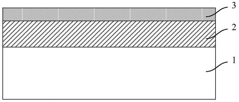
[0072] Step S1: providing a substrate, and sequentially forming a sacrificial layer and a germanium layer on the substrate;

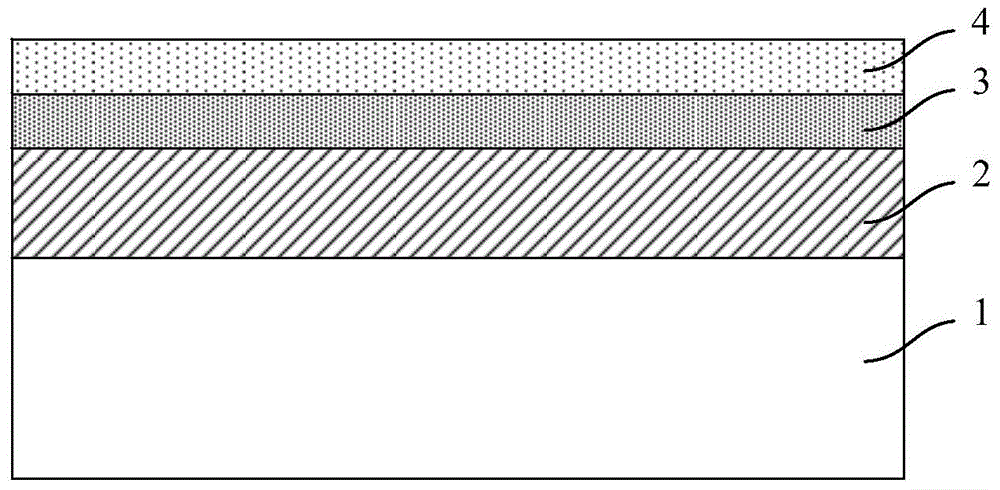
[0073] Step S2: forming a metal layer on the germanium layer, the metal layer providing stress to the germanium layer;

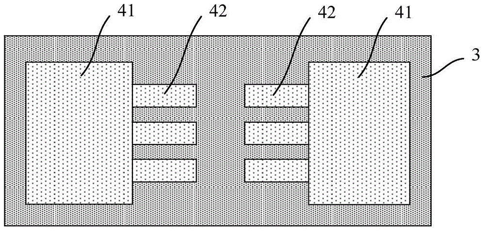
[0074] Step S3: Patterning the metal layer to form a pair of metal main bases and at least a pair of metal sub-pedestals connected to the pair of metal main bases;

[0075] Step S4: patterning the germanium layer to respectively form a germanium main pedestal and a germanium sub-pedestal under the metal main pedestal and the metal sub-pedestal, and form at least one line between each pair of germanium sub-pedestals Germanium bridge wire;

[0076] Step S5: Etching away the sacrificial layer below the germanium bridge line and the germanium sub-pedestal, so that the germanium bridge line and ...

Embodiment 2

[0093] This embodiment adopts basically the same technical solution as Embodiment 1, except that in this embodiment, metal lines connected to the metal submount are respectively formed above the two ends of the germanium bridge line.

[0094] see Figure 7 , showing a top view of the structure of the metal lines 43 connected to the metal submount 42 respectively formed above the two ends of the germanium bridge line 33 . The metal line 43 is formed synchronously with the metal main pedestal 41 and the metal sub-pedestal 42 during the patterning process of the metal layer 4 . The width of the metal line is preferably equal to the width of the germanium bridge line.

[0095] Forming metal wires 43 above the two ends of the germanium bridge wires 33 can further reduce the shear force generated on the germanium bridge wires during the film deformation process, protect the germanium bridge wires from breaking, and improve the stability of the MSM photodetector. The metal sub-pede...

Embodiment 3

[0097] This embodiment adopts basically the same scheme as Embodiment 1 or Embodiment 2. The difference is that in Embodiment 1 and Embodiment 2, uniaxial stress-strain germanium is formed, while in this embodiment, biaxial stress-strain germanium can be formed. Straining germanium can be realized only by changing the pattern of the pattern during the patterning process of the metal layer 4 and the germanium layer 3 .

[0098] Specifically, in the step S3, the metal layer is patterned to form two pairs of metal main pedestals in the horizontal and vertical directions, and a pair of metal sub-pedestals is connected between each pair of metal main pedestals; In step S4, two vertically connected germanium bridge lines are formed between the two pairs of germanium submounts; and in the step S5, after etching, the connections of the two germanium bridge lines are in both horizontal and vertical directions Stretching, forming biaxial stress and tensile strained germanium.

[0099] ...


PUM


Abstract

The invention provides a tensile strained germanium MSM photoelectric detector and the manufacturing method thereof. The method at least comprises the steps that S1, a substrate is provided and a sacrificial layer and a germanium layer are formed on the substrate in sequence; S2, a metal layer is formed on the germanium layer, and the metal layer provides stress for the germanium layer; S3, the metal layer is patterned and a pair of metal main bases and a pair of metal sub-bases are formed; S4, the germanium layer is patterned and germanium main bases and germanium sub-bases are formed below the metal main bases and the metal sub-bases respectively, and at least one germanium bridge seam is formed between each pair of germanium sub-bases; S5, the portions, below the germanium bridge seams and below the germanium sub-bases, of the sacrificial layer are etched off so that the germanium bridge seams and the germanium sub-bases are suspended in the air, the suspended germanium sub-bases are curved under the action of the action of the metal layer to enable the germanium bridge seams to be stretched, and then the tensile strained germanium MSM photoelectric detector is obtained. According to the tensile strained germanium MSM photoelectric detector and the manufacturing method thereof, the photoelectric detection property of the MSM photoelectric detector can be improved.

Description

technical field [0001] The invention belongs to the field of photoelectric devices, and relates to a tensile strain germanium MSM photodetector and a manufacturing method thereof. Background technique [0002] Metal-semiconductor-metal photodetectors (MSM-PDs) have the advantages of fast response speed, small capacitance, simple process, planar structure and easy integration, etc. It has a wide range of applications in optical fiber communication. Since the structure of the MSM detector is two back-to-back diodes, one of the diodes is always reverse-biased during operation. Therefore, the intrinsic capacitance of the device is small and does not change much with voltage. At the same time, the MSM detector is a metal-semiconductor structure device, which has no minority carrier effect, small series resistance, and small RC time constant. ), so the response speed is high. [0003] The rapid development of silicon-based optoelectronic integration in recent years is considere...

Claims


Application Information

Patent Timeline
Patent Type & Authority Applications(China)
IPC IPC(8): H01L31/18H01L31/08H01L31/0352H01L31/0216
CPCH01L31/0352H01L31/1085H01L31/1808Y02P70/50
Inventor 狄增峰母志强郭庆磊叶林陈达张苗王曦
Owner SHANGHAI INST OF MICROSYSTEM & INFORMATION TECH CHINESE ACAD OF SCI
Why Eureka
Try Eureka