Single-layer touch screen and manufacturing method thereof and touch screen displayer

A production method and touch screen technology, applied in the direction of instrument, printed circuit manufacturing, electrical digital data processing, etc., can solve the problems of complex implementation, metal bombardment, chamber pollution, etc., to prevent signal interference, prevent sputtering, and ensure cleanliness Effect

Inactive Publication Date: 2014-08-27
BEIJING BOE OPTOELECTRONCIS TECH CO LTD
View PDF8 Cites 12 Cited by
  • Summary
  • Abstract
  • Description
  • Claims
  • Application Information

AI Technical Summary

Problems solved by technology

[0004] In the production process of the above-mentioned existing single-layer touch screen, it is difficult to align the ITO bridge 5 used at the interlaced position of the horizontal and vertical sensing electrodes in the touch screen.
If the ITO bridge 5 is replaced with a metal bridge, the alignment can be made easier, but if the ITO bridge 5 is directly replaced with a metal bridge in the prior art, there will be the following problems during preparation: the metal wiring needs to be made first 6. Then the other layers and the metal wiring 6 are made in alignment. This process will cause the metal to bombard the BM frame 2, which will cause chamber pollution
[0005] Moreover, in the production process of the existing single-layer touch screen, since the shielding ITO layer 9 needs to be produced on the back side of the substrate 1, a flipping process is required, and the realization is relatively complicated.
[0006] In addition, five mask plates are required in the entire production process of the existing single-layer touch screen: mask plate 1 for forming the BM frame 2, mask plate 2 for forming the ITO bridge 5, and mask plate 2 for forming the insulating layer. 4 mask plate 3, the mask plate 4 forming the ITO electrode layer 3, and the mask plate 5 forming the protective layer 7, the cost is relatively high

Method used


Image

  • Single-layer touch screen and manufacturing method thereof and touch screen displayer
  • Single-layer touch screen and manufacturing method thereof and touch screen displayer
  • Single-layer touch screen and manufacturing method thereof and touch screen displayer

Examples


Embodiment Construction
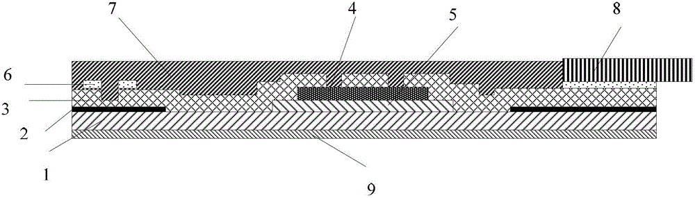
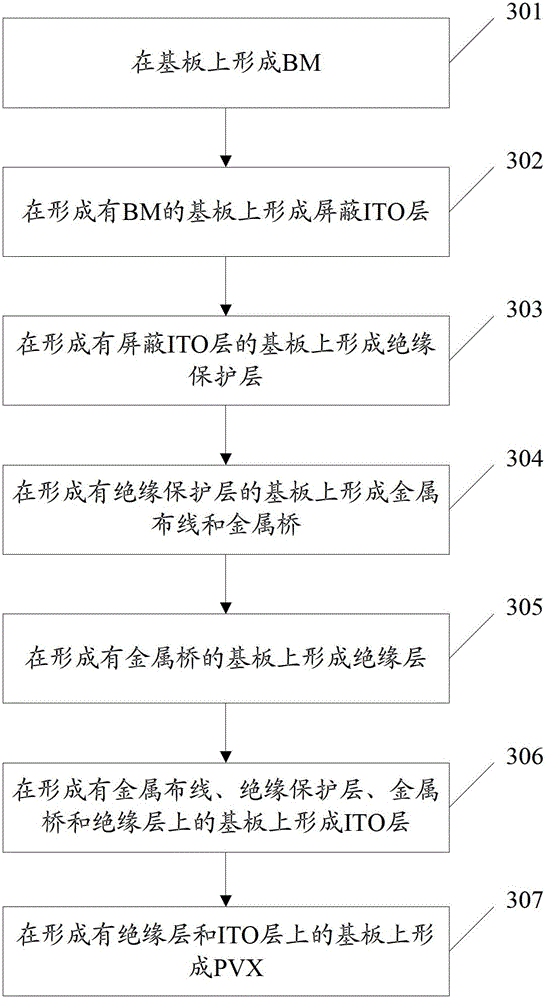
[0034] The basic idea of ​​the present invention is: in order to prevent the sputtering of the metal on the black matrix frame and ensure the cleanliness of the chamber, during the production process of the single-layer touch screen, at least above the black matrix frame and below the metal wiring , set the insulating protective layer.

[0035] Preferably, the shielding indium tin oxide layer and the frame of the black matrix are arranged on the same side of the substrate.

[0036] Preferably, at least one of the indium tin oxide electrode layer and the shielding indium tin oxide layer is disposed above the black matrix frame.

[0037] Further, the indium tin oxide electrode layer and the metal wiring are disposed above the black matrix frame via the insulating protection layer.

[0038] The present invention will be described in further detail below in conjunction with the accompanying drawings and specific embodiments.

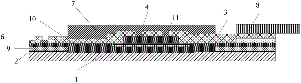
[0039] figure 2 It is a schematic structural diagr...


PUM


Abstract

Provided is a One Glass Solution touch panel, comprising: a substrate, a shielding indium tin oxide layer, a black matrix frame arranged on the substrate, metal wiring arranged above the black matrix frame, a metal bridge formed in a touch sensitive area, an insulation layer formed on the metal bridge, an indium tin oxide electrode layer arranged on the metal wiring, the metal bridge and the insulation layer, and a passivation layer arranged on the indium tin oxide electrode layer, wherein an insulation protection layer is at least arranged above the black matrix frame and below the metal wiring. Also provided at the same time are a method for manufacturing a One Glass Solution touch panel and a touchscreen display comprising the One Glass Solution touch panel. According to this disclosure, in the process of manufacturing the touchscreen, when each of the other layers is manufactured with the position thereof being aligned with the metal wiring, the sputtering of a BM by a metal can be prevented, thereby ensuring the cleanliness of a chamber.

Description

technical field [0001] The invention relates to touch screen technology in the field of liquid crystal display technology, in particular to a single-layer touch screen (One Glass Solution Touch Panel), a manufacturing method thereof, and a touch screen display. Background technique [0002] At present, due to the rapid development of the touch screen display, it has gradually developed into a mainstream flat panel display. Since its appearance, touch screen displays are mainly divided into the following three types according to their structure: Out Cell Touch Panel, On Cell Touch Panel and In Cell Touch Panel. Most of the current mainstream touch screens adopt the plug-in structure design. With the continuous improvement of the optical and electrical characteristics required by touch screen displays, and the continuous demand of consumers for thinner displays, in a limited space and with the same display effect, it is necessary to design a high-performance, low-cost , Ultr...

Claims


Application Information

Patent Timeline
Patent Type & Authority Applications(China)
IPC IPC(8): G06F3/041G02F1/1333
CPCG06F3/044G06F3/0443G06F2203/04103G06F2203/04111Y10T29/49149H05K3/1216H05K7/02
Inventor 刘英明王海生杨盛际邓立广段亚锋
Owner BEIJING BOE OPTOELECTRONCIS TECH CO LTD
Why Eureka
Try Eureka