
Integrated circuit chip with level shift LDMOS embedded in junction terminal and manufacturing method thereof

A level shift, integrated circuit technology, applied in circuits, semiconductor/solid-state device manufacturing, electrical components, etc., can solve problems such as reduced reliability and reduced device withstand voltage

Active Publication Date: 2014-09-03
CSMC TECH FAB2 CO LTD
View PDF5 Cites 8 Cited by
  • Summary
  • Abstract
  • Description
  • Claims
  • Application Information

AI Technical Summary

Problems solved by technology

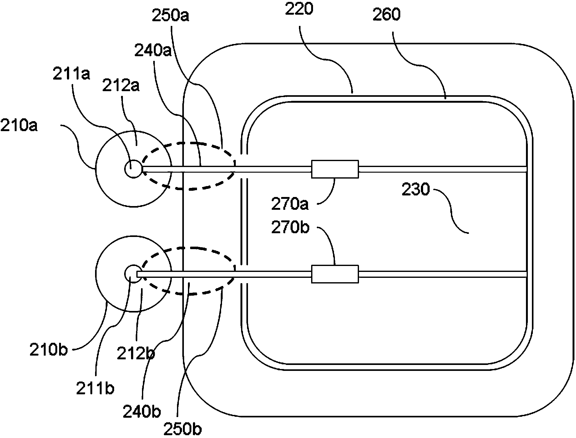
Since the potential of the metal interconnection lines 240a, 240b is a floating potential, usually several volts to hundreds of volts, the metal interconnection lines 240a, 240b will affect the electric field distribution of the semiconductors in the regions 250a, 250b they cross, which will lead to device resistance. drop in voltage, drop in reliability

Method used


Image

  • Integrated circuit chip with level shift LDMOS embedded in junction terminal and manufacturing method thereof
  • Integrated circuit chip with level shift LDMOS embedded in junction terminal and manufacturing method thereof
  • Integrated circuit chip with level shift LDMOS embedded in junction terminal and manufacturing method thereof

Examples


Embodiment 1

[0042] Figure 5 is an example along Figure 4 The cross-sectional view of the A-B line in the middle includes the P-type substrate 500, the N-type buried layer region in the P-type substrate 500, the P-type depletion region 503a in the P-type substrate 500, the P-type buried layer 503b, and the P-type substrate P-type epitaxial layer 504 on 500, N-type drift region 505a in P-type epitaxial layer 504, shifted N-well 506a, high-basin N-well 506b, high-basin P-well 507c, and displacement on P-type depletion region 503a The isolated P well 507b on the P well 507a and the P-type buried layer 503b shifts the P-type body region 511 (P+ type in this embodiment) and the N-type source region 510a (N+ type in this embodiment) in the P well 507a. type), the N-type drain region 510b (N+ in this embodiment) in the displaced N well 506a, and the bootstrap N region 510c (N+ in this embodiment) in the high-basin N well 506b.

[0043] Specifically, the aforementioned N-type buried layer regi...

Embodiment 2

[0078] Figure 7 It is the second edge of the embodiment Figure 4 The cross-sectional view of the A-B line in the middle includes the P-type substrate 700, the N-type buried layer region in the P-type substrate 700, the P-type depletion region 703a in the P-type substrate 700, the P-type buried layer 703b, and the P-type substrate P-type epitaxial layer 704 on 700, N-type drift region 705a, N-type region 705b, N-type region 705c, high-basin N well 706b, shifted N-well 706a, high-basin P well 707c, The shifted P well 707a on the P-type depletion region 703a, the isolated P well 707b on the P-type buried layer 703b, the shifted P-type body region 711 and the N-type source region 710a in the P-well 707a, and the shifted N-well 706a N-type drain region 710b inside, bootstrap N region 710c in high basin N well 706b, isolation structures 708a, 708b, 708c and 708d, first polysilicon field plate 709, dielectric layer 712, first metal field plate 713a , the second metal field plate ...

Embodiment 3

[0082] Figure 9 is the embodiment of three along Figure 4 The cross-sectional view of the A-B line in the middle includes the P-type substrate 900, the N-type buried layer region in the P-type substrate 900 (specifically including the deep buried layer 901a and the shallow buried layer 902a of the terminal N-type buried layer, and the high-basin N-type buried layer Deep buried layer 901b and shallow buried layer 902b), P-type depletion region 903a, P-type buried layer 903b in P-type substrate 900, P-type epitaxial layer 904 on P-type substrate 900, P-type epitaxial layer 904 N-type drift region 905a, N-type region 905b, N-type region 905c, high-basin N-well 906b, shifted N-well 906a, high-basin P-well 907c, shifted P-well 907a on P-type depletion region 903a, The isolated P well 907b on the P-type buried layer 903b, the P-type body region 911 and the N-type source region 910a in the shifted P-well 907a, the N-type drain region 910b in the shifted N-well 906a, and the high-b...


PUM


Abstract

The invention relates to an integrated circuit chip with a level shift LDMOS embedded in a junction terminal. The integrated circuit chip comprises the junction terminal located on the periphery of the chip, a high basin region surrounded by the junction terminal and a bootstrap level region arranged between the junction terminal and the high basin region. The level shift LDMOS is embedded in the junction terminal. The integrated circuit chip further comprises an isolating ring and a metal interconnection line. The level shift LDMOS and the junction terminal are isolated by the isolating ring. The metal interconnection line starts from the drain electrode of the level shift LDMOS, goes across a part of the junction terminal, the isolating ring and the high basin region and then is connected to the bootstrap level region. The invention further relates to a manufacturing method of the integrated circuit chip with the level shift LDMOS embedded in the junction terminal. According to the integrated circuit chip, since the voltage on the metal interconnection line is small, the influence on the region which the metal interconnection line goes across is small, and the influence on a withstand voltage is also small. Besides, due to the fact that the level shift LDMOS is embedded in the high-voltage junction terminal, the area of the high-voltage junction terminal is fully utilized, and the area of the chip can be saved.

Description

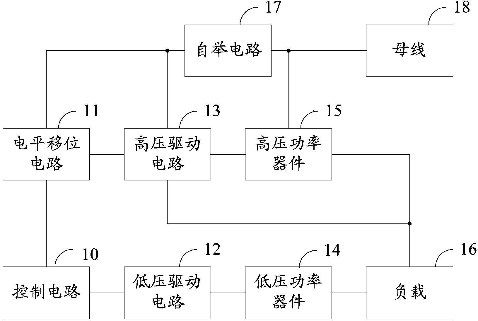
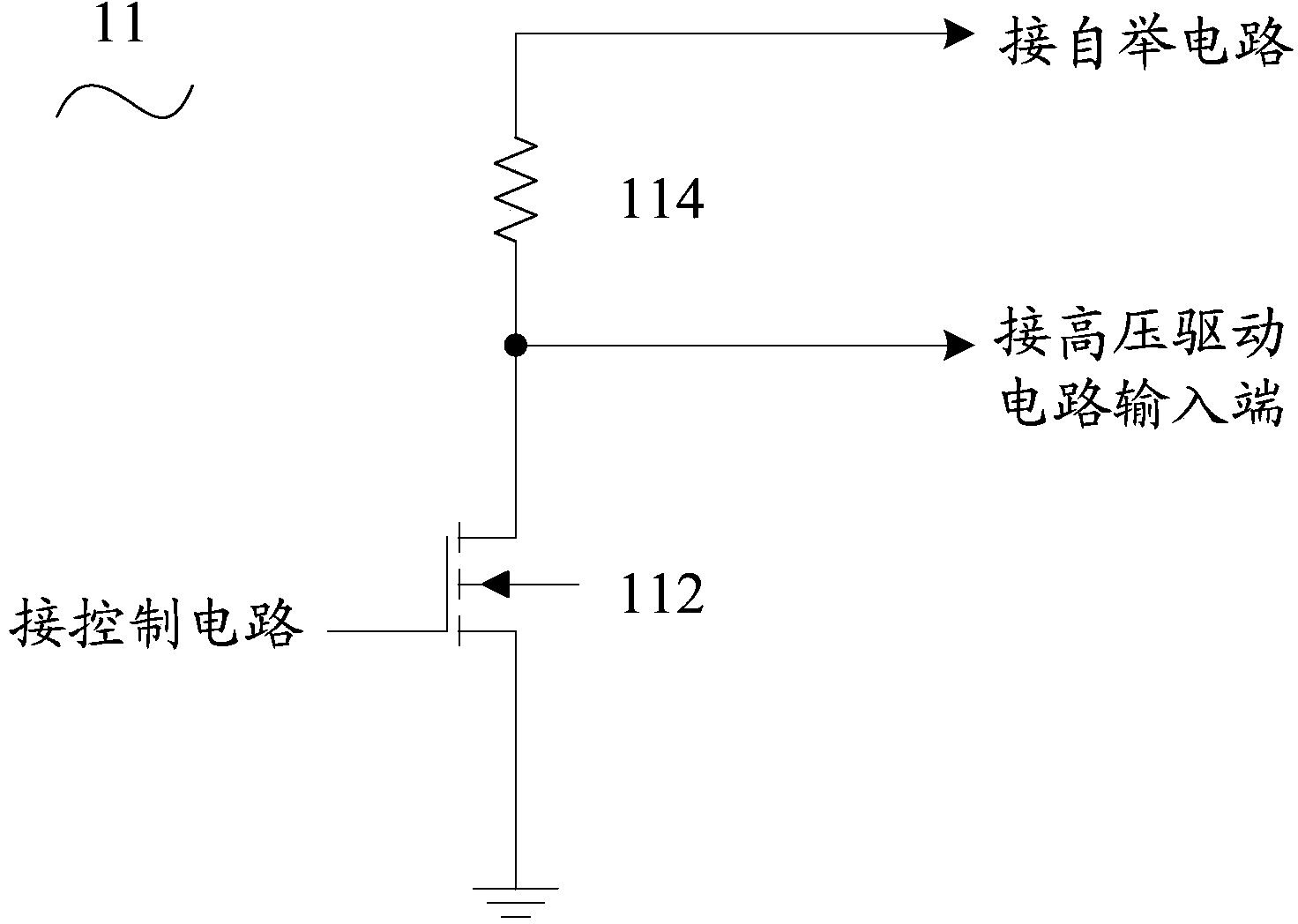
technical field [0001] The present invention relates to a semiconductor device, in particular to an integrated circuit chip with a level-shifted LDMOS embedded in a junction terminal, and a manufacturing method for an integrated circuit chip with a level-shifted LDMOS embedded in a junction terminal. Background technique [0002] A high-voltage integrated circuit usually includes a control circuit, a low-voltage drive circuit, a high-voltage drive circuit, and a level shift circuit that transmits the low-voltage control signal of the control circuit to the high-voltage drive circuit. The potential of the high-voltage drive circuit is a floating potential, usually surrounded by high-voltage junction terminals to withstand high voltage, and to isolate the high-voltage drive circuit from the low-voltage drive circuit. To pass the signal to the high-voltage driver circuit, the level-shift circuit needs to be connected to the high-voltage driver circuit. A common implementation ...

Claims


Application Information

Patent Timeline
IPC IPC(8): H01L27/02H01L29/78H01L29/06H01L29/40H01L21/82
Inventor 张森顾力晖张国华
Owner CSMC TECH FAB2 CO LTD
Learn More