Symmetric integrated stacked transformer

An integrated layer and transformer technology, applied in the direction of electric solid-state devices, semiconductor devices, semiconductor/solid-state device components, etc., can solve the problems of induction coil asymmetry, low resonance frequency, large parasitic capacitance and parasitic resistance, etc., to achieve gain and bandwidth The effect of improving and improving the quality factor and high magnetic induction coefficient

Inactive Publication Date: 2014-09-10
JIANGSU UNIV OF SCI & TECH
View PDF3 Cites 6 Cited by
  • Summary
  • Abstract
  • Description
  • Claims
  • Application Information

AI Technical Summary

Problems solved by technology

[0003] 1) The induction coil is asymmetrical and is not suitable for use in a symmetrical broadband circuit (such as a broadband fully differential amplifier) ​​to suppress common-mode signals;
[0004] 2) The parasitic capacitance of the induction coil relative to the substrate is large, because the size (or area) of the integrated laminated transformer with a high turns ratio is large (its outer diameter is generally greater than 200 μm), so both the parasitic capacitance and the parasitic resistance Larger (the parasitic capacitance of the secondary coil relative to the substrate is generally greater than 0.1pF, and the parasitic resistance of the secondary coil is generally greater than 20Ω), resulting in a lower resonance frequency (generally lower than 4GHz), which limits the integrated stacking to a certain extent Transformer performance and operating frequency range;
[0005] 3) There is no center tap, so there is only one set of outputs, and the application is limited

Method used


Image

  • Symmetric integrated stacked transformer
  • Symmetric integrated stacked transformer
  • Symmetric integrated stacked transformer

Examples


Embodiment Construction

[0024] In order to deepen the understanding of the present invention, the present invention will be described in further detail below in conjunction with the examples and accompanying drawings. The examples are only used to explain the present invention, and do not constitute regulations on the protection scope of the present invention.

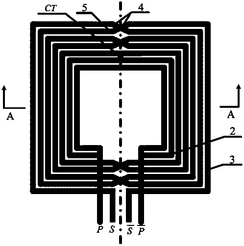
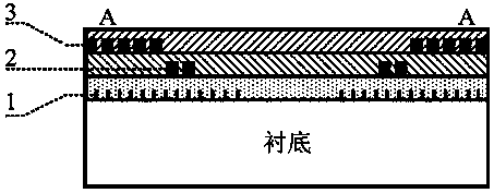
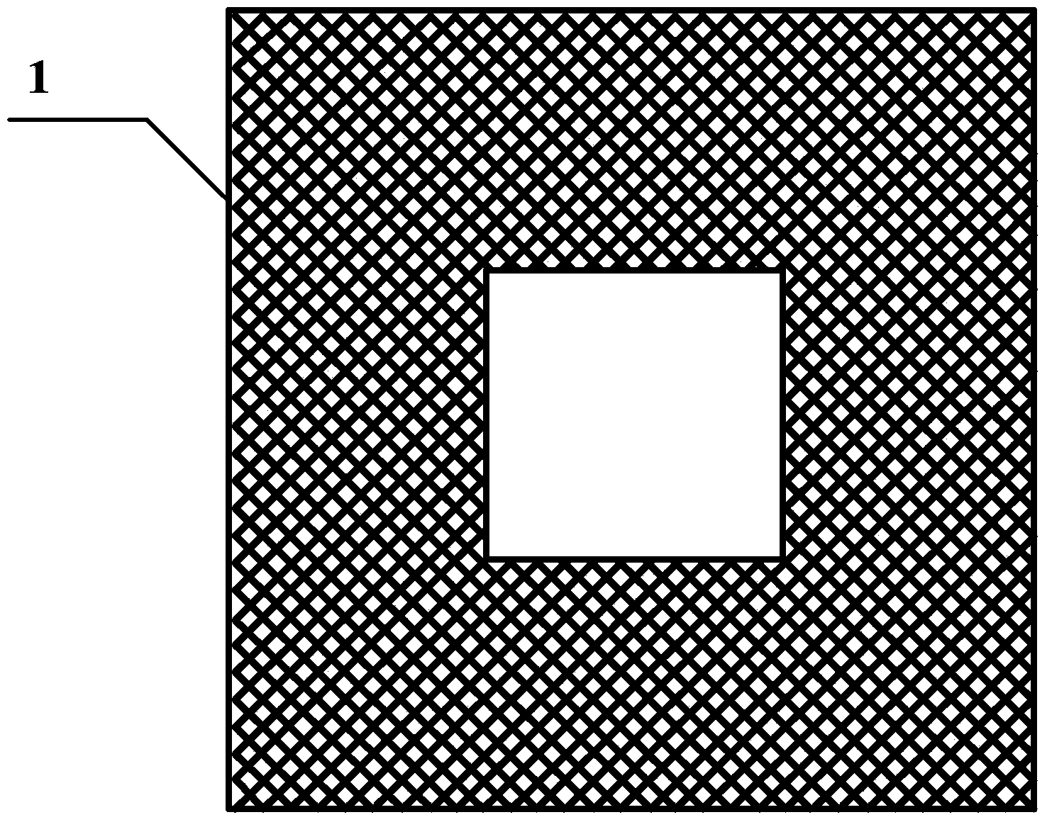
[0025] Such as figure 1 , figure 2 with image 3 As shown, a symmetrical integrated laminated transformer consists of a substrate, the first to third layers of dielectrics arranged on the substrate from bottom to top, and the shield grid 1 and the second layer respectively placed in the first layer of dielectric The primary coil 2 in the layer medium and the secondary coil 3 in the third layer medium. Wherein, the substrate is 100 μm gallium arsenide GaAs, and three layers of dielectrics are arranged on the substrate, wherein the first layer of dielectrics is silicon tetranitride Si 3 N 4 , the second dielectric layer is silicon dioxide ...


PUM


Abstract

The invention discloses a symmetric integrated stacked transformer. The symmetric integrated stacked transformer comprises a substrate, a first layer of medium, a second layer of medium and a third layer of medium, which are arranged on the substrate from bottom to top in sequence, a latticed shield grid, which is positioned in the first layer of medium, a primary coil, which is positioned in the second layer of medium, and a secondary coil, which is positioned in the third layer of medium, wherein the shield grid is arranged on the lower plane of the first layer of medium; the primary coil is formed by parallel connection of two circles of square micro-strip coils, which are separated with each other and are symmetrical around the axis, and is arranged on the lower plane of the second layer of medium; the secondary coil is formed by series connection of fives circles of square micro-strip coils, which are separated with each other and are symmetrical around the axis, and is arranged on the lower plane of the third layer of medium; the adjacent coils in pairs are crossly connected with each other at the places close to the axis through two connecting lines, one remaining circle of the coil is directly connected at the place close to the axis through the connecting line of the same metal layer, and a center tap of the secondary coil is arranged on the middle point of the coil. The symmetric integrated stacked transformer has the characteristics of good symmetry, high rate of turn and high magnetic induction coefficient.

Description

technical field [0001] The invention belongs to the technical field of radio frequency analog integrated circuits. It relates to a transformer, and more particularly relates to a symmetrical integrated laminated transformer. The invention is mainly applied in the broadband low-noise amplifier or mixer at the front end of the radio frequency receiver to convert the current or voltage of the radio frequency signal. Background technique [0002] Integrated transformers in radio frequency and microwave integrated circuits can be implemented in tiled, interleaved, and stacked types, among which the stacked type has the largest magnetic inductance. Such as literature [1] J.R.Long, "Monolithic transformers for silicon RF IC design", IEEE Journal of Solid-State Circuits, 35(9), pp.1368-1382, 2000 and literature [2] J.J.Zhou, "Monolithic transformers and their application in a differential CMOS RFlow-noise amplifier", IEEE Journal of Solid-State Circuits, 33(12), pp.2020-2027, 1998...

Claims


Application Information

Patent Timeline
Patent Type & Authority Applications(China)
IPC IPC(8): H01L23/522
Inventor 李效龙杨奕飞张贞凯田雨波解志斌王彪张冰
Owner JIANGSU UNIV OF SCI & TECH
Why Eureka
Try Eureka