Semiconductor structure and forming method thereof

A semiconductor and conductor technology, applied in the field of ultra-large-scale integrated circuit manufacturing, can solve problems such as complex processes, and achieve the effects of large process window, process compatibility, and low process cost.

Active Publication Date: 2014-09-10
PEKING UNIV
View PDF6 Cites 4 Cited by
  • Summary
  • Abstract
  • Description
  • Claims
  • Application Information

AI Technical Summary

Problems solved by technology

However, the quality and thickness of each layer of film in the superlattice structure are limited by factors such as lattice mismatch and stress release, and the process is relatively complicated.

Method used


Image

  • Semiconductor structure and forming method thereof
  • Semiconductor structure and forming method thereof
  • Semiconductor structure and forming method thereof

Examples


Embodiment 1

[0068] A two-layer circular nanowire structure with a diameter of about 10 nm can be achieved according to the following steps:

[0069] 1) Thermal growth on (111) bulk silicon substrate SiO 2 As a stress buffer layer between the hard mask and the silicon substrate;

[0070] 2) LPCVD Si 3 N 4 as an etch hard mask;

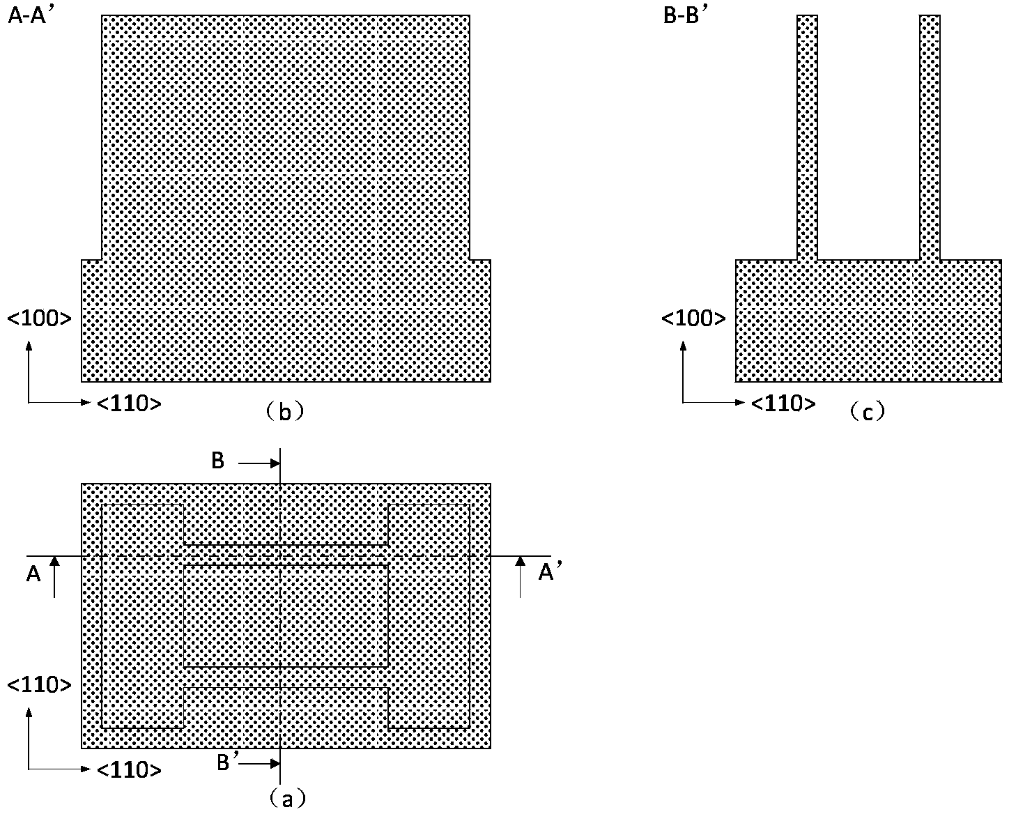
[0071] 3) Define Fin and the source and drain regions connected to both ends of Fin on the hard mask by photolithography, wherein the width of the Fin structure is 20nm, the length is 300nm, and the length direction and the sidewall crystal direction are both along ;

[0072] 4) Transfer the pattern to the hard mask by anisotropic etching to expose the silicon substrate;

[0073] 5) Transfer the pattern on the hard mask to the silicon substrate by anisotropic etching to form Fin and the source and drain regions connected to both ends of Fin, wherein the height of the Fin structure is The width is 20nm, the length is 300nm, and the length direction and sid...

Embodiment 2

[0097] A two-layer square nanowire structure with a diameter of about 5 nm can be achieved according to the following steps:

[0098] 1) Thermal growth on (100) bulk silicon substrate SiO 2 As a stress buffer layer between the hard mask and the silicon substrate;

[0099] 2) LPCVD Si 3 N 4 as an etch hard mask;

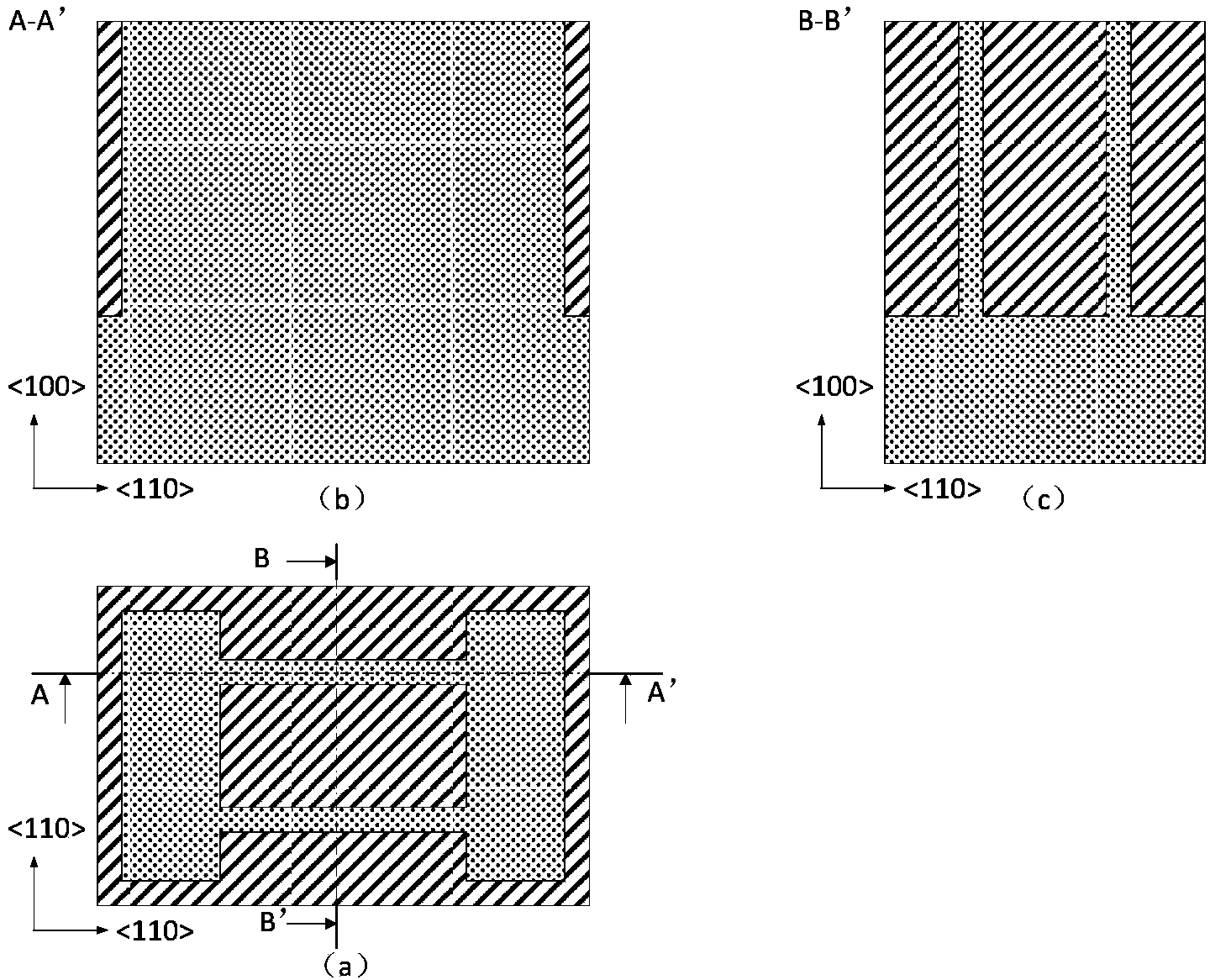
[0100] 3) Define Fin and the source and drain regions connected to both ends of Fin on the hard mask by photolithography. The width of the Fin structure is 10nm, the length is 300nm, the length direction is along , and the sidewall crystal directions are all along ;

[0101] 4) Transfer the pattern to the hard mask by anisotropic etching to expose the silicon substrate;

[0102] 5) Transfer the pattern on the hard mask to the silicon substrate by anisotropic etching to form Fin and the source and drain regions connected to both ends of Fin, wherein the height of the Fin structure is The width is 10nm, the length is 300nm, the length direction is along , and ...

Embodiment 3

[0125] A three-layer nanowire structure with a diameter of about 10 nm was prepared.

[0126] 1) Thermal growth on (110) bulk silicon substrate SiO 2 As a stress buffer layer between the etched hard mask and the silicon substrate;

[0127] 2) LPCVD Si 3 N 4 as an etch hard mask for silicon;

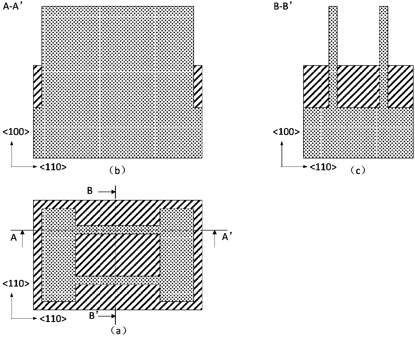
[0128] 3) Define Fin and the source and drain regions connected to both ends of Fin by photolithography, wherein the width of the Fin structure is 30 nanometers, the length is 300 nanometers, the length direction is along the crystal direction, and the side wall is along the crystal direction;

[0129] 4) Transfer the pattern to the hard mask by anisotropic etching to expose the silicon substrate;

[0130] 5) Transfer the pattern on the hard mask to the silicon substrate by anisotropic etching to form Fin and the source and drain regions connected to both ends of Fin, wherein the height of the Fin structure is The width is 30 nanometers, the length is 300 nanometers, the lengt...


PUM

PropertyMeasurementUnit
widthaaaaaaaaaa
lengthaaaaaaaaaa
widthaaaaaaaaaa

Abstract

A semiconductor structure comprises a semiconductor substrate and multiple layers of superfine silicon lines. Interface shapes of the multiple layers of superfine silicon lines are doubly controlled by a crystal orientation of the substrate and axial crystal orientations of the lines. A forming method of the semiconductor structure includes: forming a fin-shaped silicon island Fin and source drain areas at two ends of the silicon island via an etching technology; preparing a corrosion masking layer for silicon; forming multiple layers of superfine silicone lines. The semiconductor structure and the forming method there of have the advantages that the finally formed multiple layers of superfine silicon lines are uniform and controllable in positions and section shapes; self-stopping of aeolotropism corrosion, large technical windows and the silicon lines in different diameters on a same silicon slice are achieved; ICPECVD (inductively coupled plasma enhance chemical vapor deposition) is strong in narrow groove filling power, and no cavity is left when materials of a sacrificial layer and the corrosion masking layer are deposited; the lines smaller than 10nm in size can be prepared by combining an oxidization technology, requirements on key technologies for small-size devices are met; a processing method is implemented from top to bottom and compatible with a bulk silicon planar transistor technology, and technical cost is low.

Description

technical field [0001] The invention belongs to the technical field of ultra-large-scale integrated circuit manufacturing, and relates to a structure of multilayer ultra-fine silicon lines and a preparation method thereof, in particular to a side wall mask technology combining fin-shaped silicon islands and anisotropic etching of silicon Technology to prepare multi-layer ultra-fine silicon lines with controllable position and shape. Background technique [0002] As Moore's Law advances to the 22nm process node, traditional planar devices have become increasingly prominent due to short-channel effects and reliability issues, resulting in serious degradation of device performance and failing to meet the requirements of Moore's Law. The three-dimensional multi-gate device (Multi-gate MOSFET, MuGFET) represented by the fin field effect transistor (FinFET), with its outstanding ability to suppress the short channel effect, high integration density, and compatibility with traditio...

Claims


Application Information

Patent Timeline
Patent Type & Authority Applications(China)
IPC IPC(8): H01L23/528H01L21/768
CPCH01L2924/0002H01L21/02238H01L21/30604H01L21/30608H01L21/3083B82Y10/00B82Y40/00H01L29/66439H01L29/775H01L29/78696H01L29/045H01L29/0673H01L29/42392H01L2924/00H01L21/02236H01L21/02271H01L21/0274H01L21/31055H01L29/66795H01L29/785
Inventor 黎明杨远程樊捷闻宣浩然张昊黄如
Owner PEKING UNIV
Why Eureka
Try Eureka