

Metal thin film for electronic component and mo alloy sputtering target material for forming metal thin film
A metal thin film and sputtering target technology, which is applied in the field of sputtering targets, can solve problems such as low adhesion, achieve improved reliability, excellent oxidation resistance, and contribute to the effect of stable manufacturing
- Summary
- Abstract
- Description
- Claims
- Application Information
AI Technical Summary
Problems solved by technology
Method used
Image

Examples
Embodiment 1
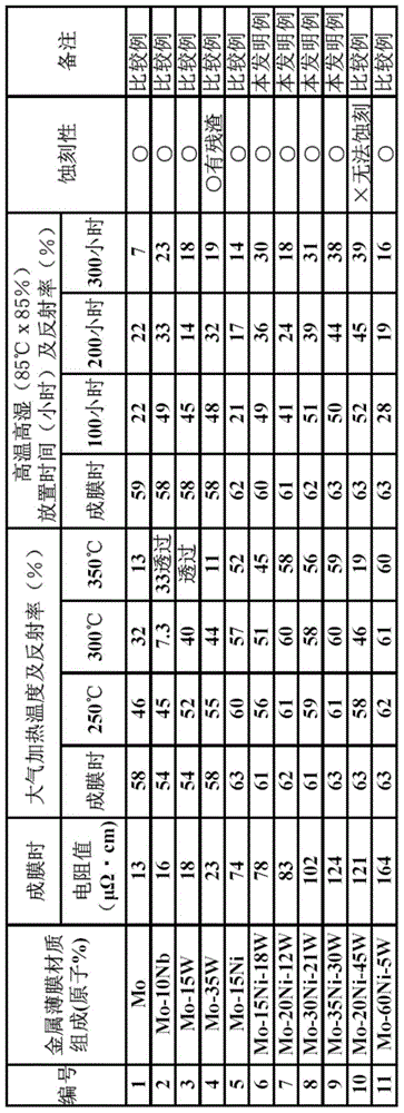
[0053] First, each sputtering target for forming the metal thin film for electronic components was produced. Mo powder with an average particle diameter of 6 μm, Ni powder with an average particle diameter of 100 μm, and W powder with an average particle diameter of 8 μm were prepared. Next, the above-mentioned powders were mixed and filled into mild steel tanks so as to form Mo-30 atomic % Ni alloy and Mo-35 atomic % W alloy, and then vacuum exhausted while heating to remove the gas in the tank. Seal after ingredients. Next, the sealed can was placed in a hot isostatic press, and after sintering at 1000° C., 120 MPa, for 5 hours, each sputtering target with a diameter of 100 mm and a thickness of 5 mm was produced by machining.
[0054] In addition, sputtering targets composed of Mo-10 atomic % Nb alloy, Mo-15 atomic % Ni alloy, and Mo-15 atomic % W were produced in the same manner.
[0055] In addition, the sputtering target of the Ni-20 atomic % W alloy was produced by we...
Embodiment 2
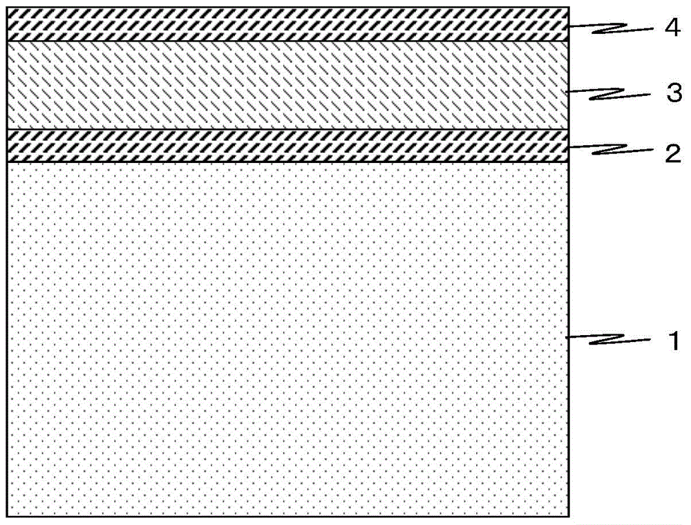
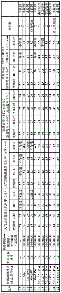
[0069] conceived as figure 1 For the configuration of the laminated wiring film shown, the base film with the composition shown in Table 2 was formed on a glass substrate of 25 mm x 50 mm, and the base film was formed with the film thickness shown in Table 2 using the same sputtering device as in Example 1. A Cu film as a main conductive film was formed on the upper surface of the Cu film, and a cover film having the composition shown in Table 2 was formed on the Cu film to obtain a sample of a laminated wiring film. Among them, the Cu sputtering target was manufactured by machining an oxygen-free copper plate of Hitachi Electric Wire Co., Ltd.
[0070] Evaluation of oxidation resistance was measured under the same conditions as in Example 1. In addition, regarding the evaluation of the moisture resistance, changes in the resistance value after leaving each sample obtained above in a high-temperature, high-humidity environment of 85° C.×85% for 100 hours and 200 hours were m...
Embodiment 3
[0079] In the same manner as in Example 2, an undercoat film having the composition shown in Table 3 was formed on a glass substrate of 25 mm×50 mm, and formed on the undercoat film with the film thickness shown in Table 3 using the same sputtering device as in Example 1. An Al film of the main conductive film, and further a cover film was formed on the Al film to obtain a sample of a laminated wiring film. Among them, the sputtering target of Al was manufactured by machining a plate purchased from Sumitomo Chemical Co., Ltd.
[0080] Evaluation of oxidation resistance was measured under the same conditions as in Example 1. In addition, regarding the evaluation of moisture resistance, changes in resistance value were measured after leaving each sample obtained above in a high-temperature and high-humidity environment of 85° C.×85% for 100 hours, 200 hours, and 300 hours. The resistance value was measured using a 4-terminal thin film resistivity meter MCP-T400 manufactured by ...
PUM
| Property | Measurement | Unit |
|---|---|---|
| Diameter | aaaaa | aaaaa |
| Thickness | aaaaa | aaaaa |
Abstract
Description
Claims
Application Information