

Electronic tag inlay, processing method of electronic tag inlay and electronic tag
An electronic label and processing method technology, applied in the field of radio frequency identification, to achieve the effect of high strength, simple production process, convenient and quick operation
- Summary
- Abstract
- Description
- Claims
- Application Information
AI Technical Summary
Problems solved by technology
Method used
Image

Examples
Embodiment 1
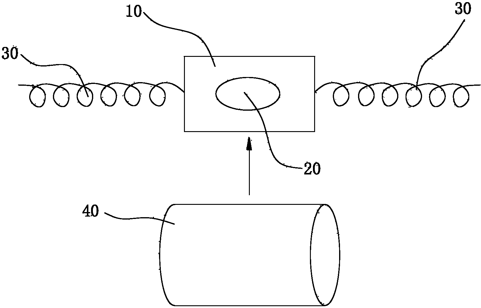
[0056] figure 1 and figure 2 Shown is an electronic tag inlay provided by Embodiment 1 of the present invention, which consists of five parts: a dielectric board 10, a chip 20, an antenna, a protective material, and a protective cover 40, wherein:
[0057] A pad is provided on the dielectric board 10; the dielectric board 10 can be made of glass fiber boards, ceramic boards, resin boards, composite boards, bakelite boards or Teflon boards (ie PTFE boards) and other boards, or other materials suitable for high-frequency signal transmission. Plate; pads can be copper etched pads;
[0058] The chip 20 and the antenna are respectively connected to the dielectric plate to realize the electrical conduction between the chip 20 and the antenna; in the present embodiment, the antenna is a spiral metal wire with a spring structure (hereinafter referred to as the spring antenna 30), and of course other such as Ordinary metal wires and other antennas made of metal structures with certa...
Embodiment 2
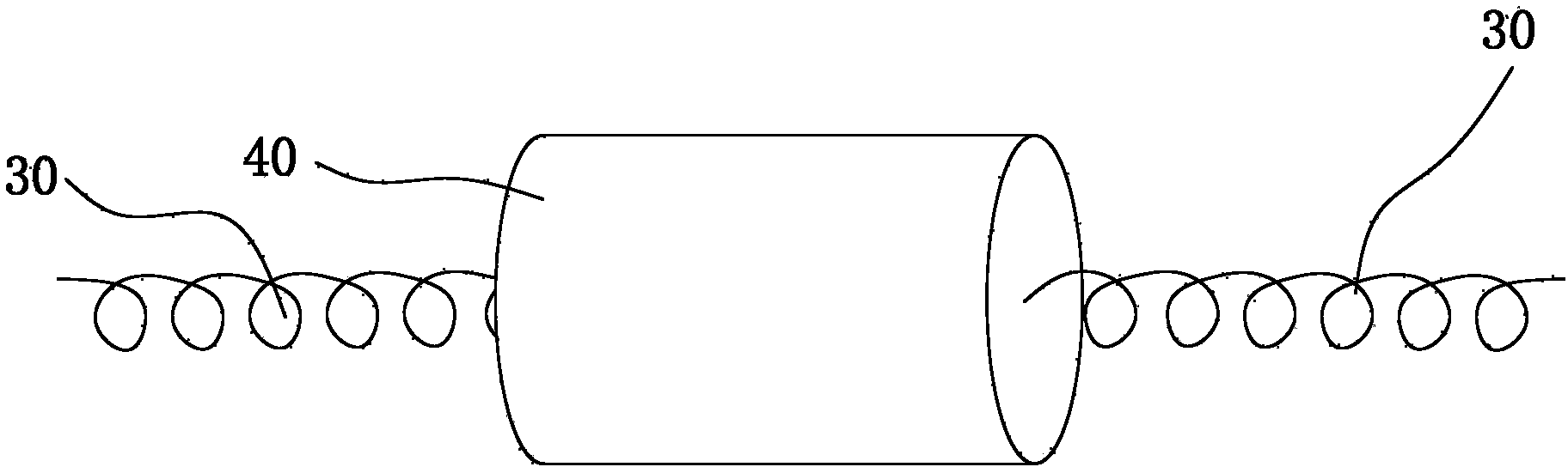
[0064] The electronic tag inlay provided in this embodiment is also composed of five parts: a dielectric board, a chip, an antenna, a protective material and a protective cover, wherein:
[0065] There is a pad on the dielectric board; the dielectric board can be made of glass fiber board, ceramic board, resin board, composite board, bakelite board or Teflon board, or other boards suitable for high-frequency signal transmission; the pad can be made of copper Etched pad;
[0066] The chip and the antenna are respectively connected to the dielectric board to realize electrical conduction between the chip and the antenna; in this embodiment, the antenna is a copper braided wire, and the copper braided wire includes two parts of equal length, which are respectively connected to both sides of the dielectric board. In this embodiment, the length of each part of the copper braided wire is about 1 / 4 of the wavelength of the radio frequency signal; the chip can be connected to the pad ...
Embodiment 3
[0072] The present embodiment provides a kind of processing method of electronic label inlay, comprises the following steps:
[0073] (1) The chip is connected to the pad of the dielectric board by using a package body with pins through gold wire or soldering tin. In other embodiments, the chip can also be directly fixed on the dielectric board through the COB process through the bare crystal.
[0074] The dielectric board can be made of glass fiber board, ceramic board, resin board, composite board, bakelite board or Teflon board, or other boards suitable for high-frequency signal transmission; the pad can be copper-etched pad.
[0075] (2) The antenna is connected to the pad of the dielectric board by welding. In other embodiments, screw holes may also be provided at both ends of the dielectric board, and the antenna is connected to the pad of the dielectric board by screw connection.
[0076]Wherein, the antenna can be a copper braided wire, a spiral metal wire with a sprin...
PUM
 Abstract
Description
Claims
Application Information