Superconductive nanowire single photon detector based on dielectric film reflector
A single-photon detector and superconducting nanowire technology, applied in the field of light detection, can solve the problems of low tolerance of nanowire size, influence of absorption efficiency, low absorption efficiency, etc., achieve large tolerance, avoid influence, and high absorption efficiency Effect
- Summary
- Abstract
- Description
- Claims
- Application Information
AI Technical Summary
Problems solved by technology
Method used
Image

Examples
Embodiment 1
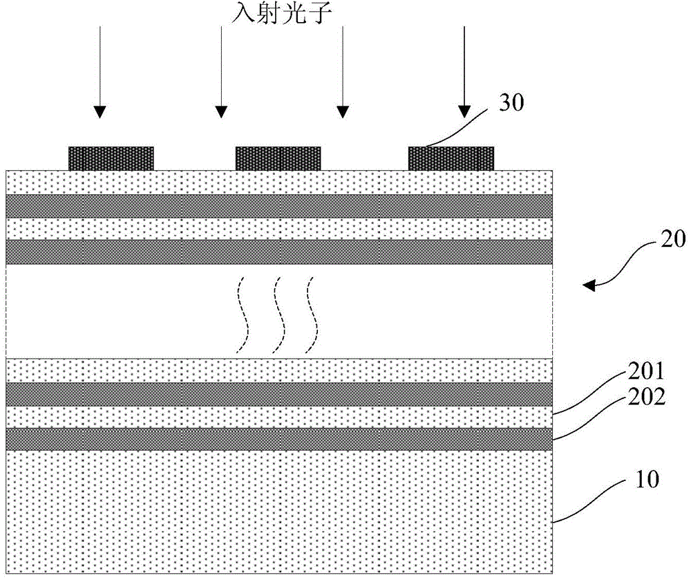
[0038] Such as image 3 As shown, this embodiment provides a superconducting nanowire single photon detector based on a dielectric film mirror, including:
[0039] Substrate 10;
[0040] An all-dielectric multilayer film reflector 20, bonded to the surface of the substrate 10;
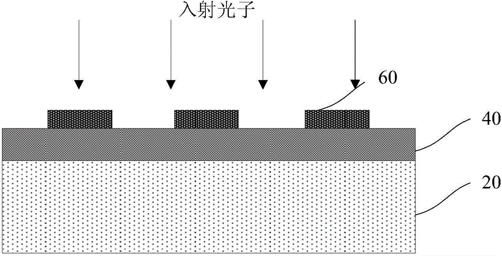
[0041] The superconducting nanowires 30 are combined on the surface of the all-dielectric multilayer film mirror 20 .
[0042] As an example, the superconducting nanowire single-photon detector based on a dielectric film mirror in this embodiment is a superconducting nanowire 30 single-photon detector with a front-incidence structure.
[0043] As an example, the substrate 10 includes a silicon substrate, an MgO substrate or a sapphire substrate, and the thickness of the substrate 10 is 300-500 microns. In this embodiment, the substrate 10 is a silicon substrate 10 with a thickness of 400 microns. Of course, other types of substrates 10 or thicknesses may also be applicable to the present invention,...
Embodiment 2
[0048] Such as Figure 4 As shown, this embodiment provides a superconducting nanowire single photon detector based on a dielectric thin film mirror. 2 Layer 201 with TiO 2 layer 203, and the uppermost layer (that is, the layer in contact with the superconducting nanowire 30) is SiO 2 Layer 201. The all-dielectric multilayer film used in this embodiment benefits from mature optical film technology, is very easy to implement, and has low process cost. Using all-dielectric materials as reflectors avoids the absorption loss of light by metal materials, especially avoids the The loss of light in the infrared band, and the use of a mirror structure with the surface of the substrate 10 can avoid the influence of the Fabry-Perot cavity of the substrate 10 on the absorption efficiency.
[0049] Such as Figure 7 In the present example, the reflectivity of the dielectric film mirror and the absorption efficiency (absorptance) of the superconducting nanowire single photon detection ...
Embodiment 3
[0051] Such as Figure 5 As shown, this embodiment provides a superconducting nanowire single photon detector based on a dielectric thin film mirror. 2 Layer 201 with Ta 2 o 5 layer 204, and the uppermost layer (that is, the layer in contact with the superconducting nanowire 30) is SiO 2 Layer 201. The all-dielectric multilayer film used in this embodiment benefits from mature optical film technology, is very easy to implement, and has low process cost. Using all-dielectric materials as reflectors avoids the absorption loss of light by metal materials, especially avoids the The loss of light in the infrared band, and the use of a mirror structure with the surface of the substrate 10 can avoid the influence of the Fabry-Perot cavity of the substrate 10 on the absorption efficiency.
PUM
| Property | Measurement | Unit |
|---|---|---|
| Thickness | aaaaa | aaaaa |
| Thickness | aaaaa | aaaaa |
Abstract
Description
Claims
Application Information
 - R&D
- Intellectual Property
- Life Sciences
- Materials
- Tech Scout
- Unparalleled Data Quality
- Higher Quality Content
- 60% Fewer Hallucinations
Browse by: Latest US Patents, China's latest patents, Technical Efficacy Thesaurus, Application Domain, Technology Topic, Popular Technical Reports.
© 2025 PatSnap. All rights reserved.Legal|Privacy policy|Modern Slavery Act Transparency Statement|Sitemap|About US| Contact US: help@patsnap.com