Bulk-silicon micro electromechanical system MEMS structure front surface subsequent processing method

A micro-electro-mechanical system and process technology, applied in the direction of micro-structure technology, micro-structure devices, manufacturing micro-structure devices, etc., can solve the problems of low product qualification rate and easy damage of suspended structures, so as to strengthen the suspended structure, facilitate product design and Typesetting, the effect of improving utilization

Active Publication Date: 2014-10-15
SHANGHAI INTEGRATED CIRCUIT RES & DEV CENT
View PDF5 Cites 2 Cited by
  • Summary
  • Abstract
  • Description
  • Claims
  • Application Information

AI Technical Summary

Problems solved by technology

[0005] The invention aims to solve the problem that when the micro-electromechanical system MEMS is processed on the front side after the bulk silicon structure is formed, the formed suspended structure is easy to be damaged and the product qualification rate is low

Method used


Image

  • Bulk-silicon micro electromechanical system MEMS structure front surface subsequent processing method
  • Bulk-silicon micro electromechanical system MEMS structure front surface subsequent processing method
  • Bulk-silicon micro electromechanical system MEMS structure front surface subsequent processing method

Examples


Embodiment 1

[0024] Please refer to Figure 1A ~ Figure 1G , is a cross-sectional schematic diagram of the front-side process method of the bulk silicon micro-electromechanical system MEMS structure according to Embodiment 1 of the present invention.

[0025] In this embodiment, specific circuits on the front side of the silicon chip need to be protected, and only the area to be released is exposed. This embodiment adopts the method of photoresist protective layer.

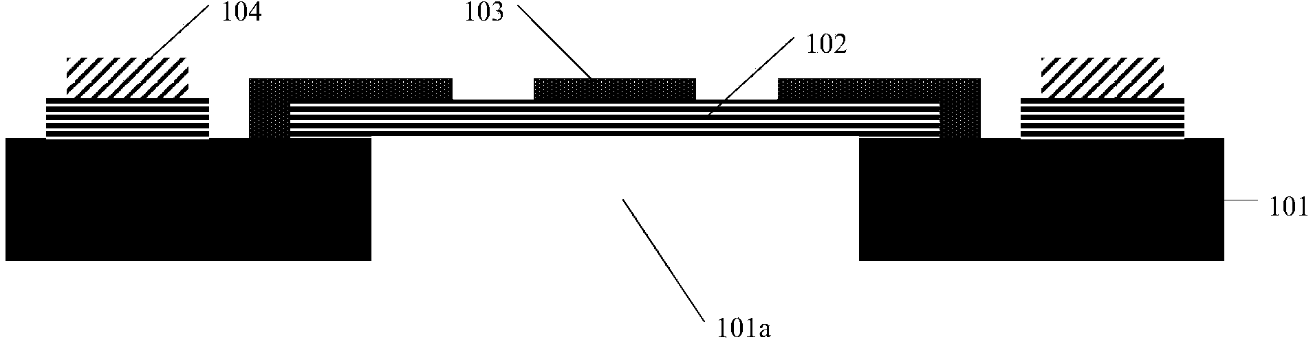
[0026] First, please refer to Figure 1A A typical bulk silicon MEMS structure is shown. Deep grooves 101a are etched from the backside of the silicon wafer 101 . From top to bottom, the front side of the silicon chip is a MEMS support and functional layer 103, and a sacrificial layer 102 between the MEMS support and functional layer 103 and the deep groove 101a. The periphery of the MEMS support and functional layer 103 is a circuit part 104, and its height is slightly above the MEMS support and functional layer 103 .

...

Embodiment 2

[0036] Please refer to Figure 2A ~ Figure 2K , is a schematic cross-sectional view of the front-side process method of the bulk silicon MEMS structure according to Embodiment 2 of the present invention.

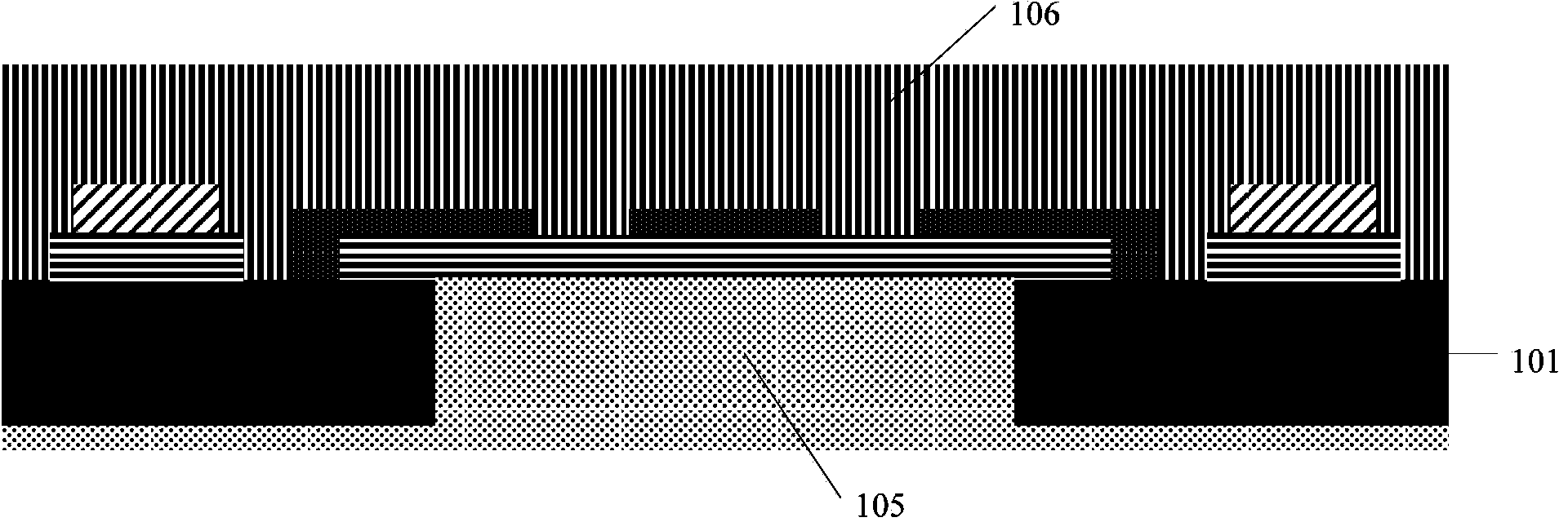
[0037] In this embodiment, a dielectric protection layer needs to be deposited on a specific line on the front side of the silicon wafer, so as to prevent further corrosion of the protected area by the release of chemical solution or reaction gas when the sacrificial layer is released.

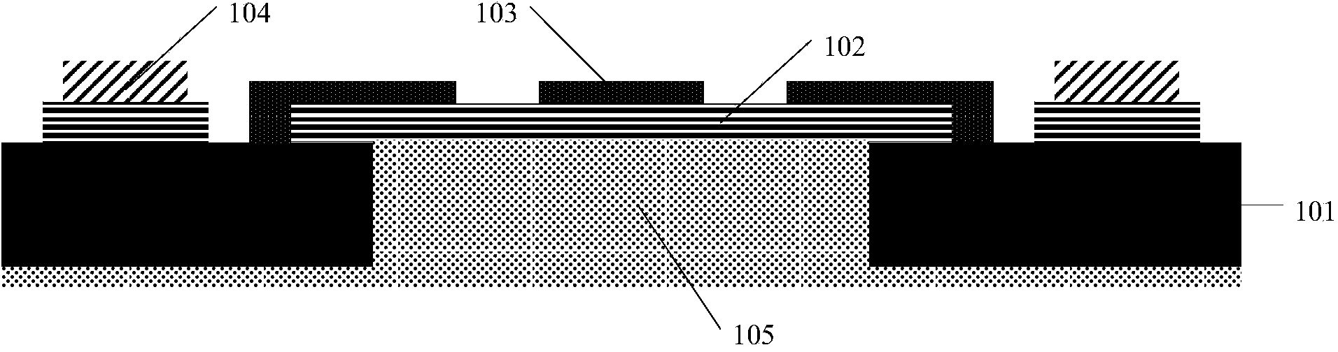
[0038] Figure 2A It is a typical bulk silicon MEMS structure. Deep trenches 201a are etched from the backside of the silicon wafer 201 . The front side of the silicon chip is MEMS support and functional layer 203 from top to bottom, and the sacrificial layer 202 between MEMS support and functional layer 203 and deep groove 201a, and the periphery of MEMS support and functional layer 203 is circuit part 204, and its height is slightly above the MEMS support and functional layer 203 .

[...

Embodiment 3

[0048] In some applications, the thin film 207 of the second embodiment is not a dielectric protection layer, but a component of a specific circuit necessary to realize a certain function. Therefore complete the example shown in the second example Figure 2A ~ Figure 2F The steps in the above step only complete the deposition and patterning of the specific circuit, and it is necessary to continue to use the photoresist protection layer to protect the specific circuit formed in the second embodiment from being damaged when the sacrificial layer is subsequently released. Embodiment 3 provides the operation method in the above situation.

[0049] Similar to the structure shown in the second embodiment, the thin film 207 is an integral part of a specific circuit necessary to realize a certain function. After the deposition and patterning of the dielectric layer 207 on the front side of the silicon wafer 201 is completed, it needs to be protected, and only the area on the front si...


PUM

PropertyMeasurementUnit
thicknessaaaaaaaaaa

Abstract

The invention discloses a bulk-silicon micro electromechanical system MEMS structure front surface subsequent processing method which includes steps of providing a bulk-silicon micro electromechanical system MEMS structure with a silicon wafer having a deep groove formed in the back surface, filling the deep groove in the back surface with photoresist, processing the front surface of the silicon wafer, releasing or removing a sacrificial layer and drying to obtain the final structure. The method is adaptable to front surface subsequent processing after the back surface of the silicon wafer of the bulk-silicon structure is formed. The method utilizing conventional semiconductor equipment is compatible with a semiconductor technique, has high technological maturity and controllability, and is low in cost, high in stability, short in operating time and applicable to large-scale production. Chip area utilization rate is increased due to the fact that no special vacuum suction area needs to be reserved on an MEMS chip. In addition, the risk of damaging the suspension structure of the MEMS caused by disturbance generated during front surface processing is reduced greatly and yield is increased.

Description

technical field [0001] The invention relates to the technical field of integrated circuits, in particular to a method for continuing the front-side process of a bulk silicon micro-electro-mechanical system MEMS structure. Background technique [0002] In the MEMS structure of bulk silicon MEMS, many holes or deep grooves are etched on the back of the silicon substrate. Due to the lack of a solid substrate supporting fulcrum, the suspended structure on the front of the silicon wafer is very weak. At this time, if the film deposition, photolithography or etching process is continued on the front of the silicon wafer, the suspended structure will easily be damaged. [0003] In order to ensure the maximum yield, the front-side process is generally completed before the bulk silicon process. After the bulk silicon structure is formed, in order to prevent damage to the suspended structure caused by mechanical disturbance, only sacrificial layer release and drying are performed with...

Claims


Application Information

Patent Timeline
Patent Type & Authority Applications(China)
IPC IPC(8): B81C1/00
Inventor 袁超
Owner SHANGHAI INTEGRATED CIRCUIT RES & DEV CENT
Why Eureka
Try Eureka