Eureka AIR delivers breakthrough ideas for toughest innovation challenges, trusted by R&D personnel around the world.

Process deviation tolerating and reading interference eliminating reading amplifying circuit

A technology for read interference and process deviation, applied in the field of read amplifying circuits, can solve the problems of increasing the input offset of the read circuit, affecting the read reliability performance, and reducing the STT-MRAM read decision margin.

Active Publication Date: 2014-11-05
致真存储(北京)科技有限公司
View PDF3 Cites 7 Cited by
  • Summary
  • Abstract
  • Description
  • Claims
  • Application Information

AI Technical Summary

Problems solved by technology

[0003] At present, the large-scale production and popularization of STT-MRAM is facing serious read reliability problems: (1) Due to the limitations of materials and manufacturing processes, the TMR value that can be obtained at room temperature is relatively small, so the available read judgment margin is relatively small. The amount is relatively small, when the read decision margin cannot overcome the device mismatch (Device Mismatch) or input offset (Input Offset) of the read circuit itself, a read error occurs; (2) The continuous shrinking of the process size leads to serious Process deviation, resulting in serious device mismatch (including the STT-MRAM memory cell itself and peripheral circuits, etc.), these factors further reduce the read decision margin of STT-MRAM, while increasing the input offset of the read circuit, affecting Read reliability performance; (3) In order to increase the read decision margin and improve the read reliability, it is necessary to provide a larger external read current, but due to the existence of the STT effect, an excessively large external current may affect the STT-MRAM The data stored in the data unit or reference unit is rewritten, causing read disturbance. It can be seen that there is a contradiction between read disturbance and read decision margin.

Method used


Image

  • Process deviation tolerating and reading interference eliminating reading amplifying circuit
  • Process deviation tolerating and reading interference eliminating reading amplifying circuit
  • Process deviation tolerating and reading interference eliminating reading amplifying circuit

Examples


Embodiment Construction

[0058] The substantive features of the present invention are further described with reference to the accompanying drawings. Embodiments disclosed herein, specific structural and functional details thereof are for the purpose of describing specific embodiments only, therefore, the present invention may be embodied in many alternative forms and the present invention should not be construed as limited only to the embodiments described herein. Instead, this presents example embodiments to cover all changes, equivalents, and alternatives falling within the scope of the invention. Additionally, well-known elements, devices and subcircuits of the invention will not be described in detail or will be omitted so as not to obscure the relevant details of the embodiments of the invention.

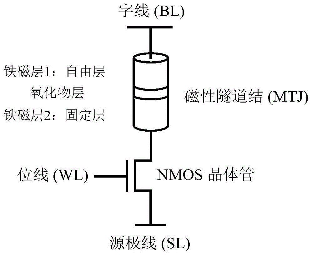
[0059] figure 1 It is a structural schematic diagram of an STT-MRAM memory cell using the reading circuit of the present invention.

[0060] The STT-MRAM memory cell consists of a magnetic tunnel jun...


PUM


Abstract

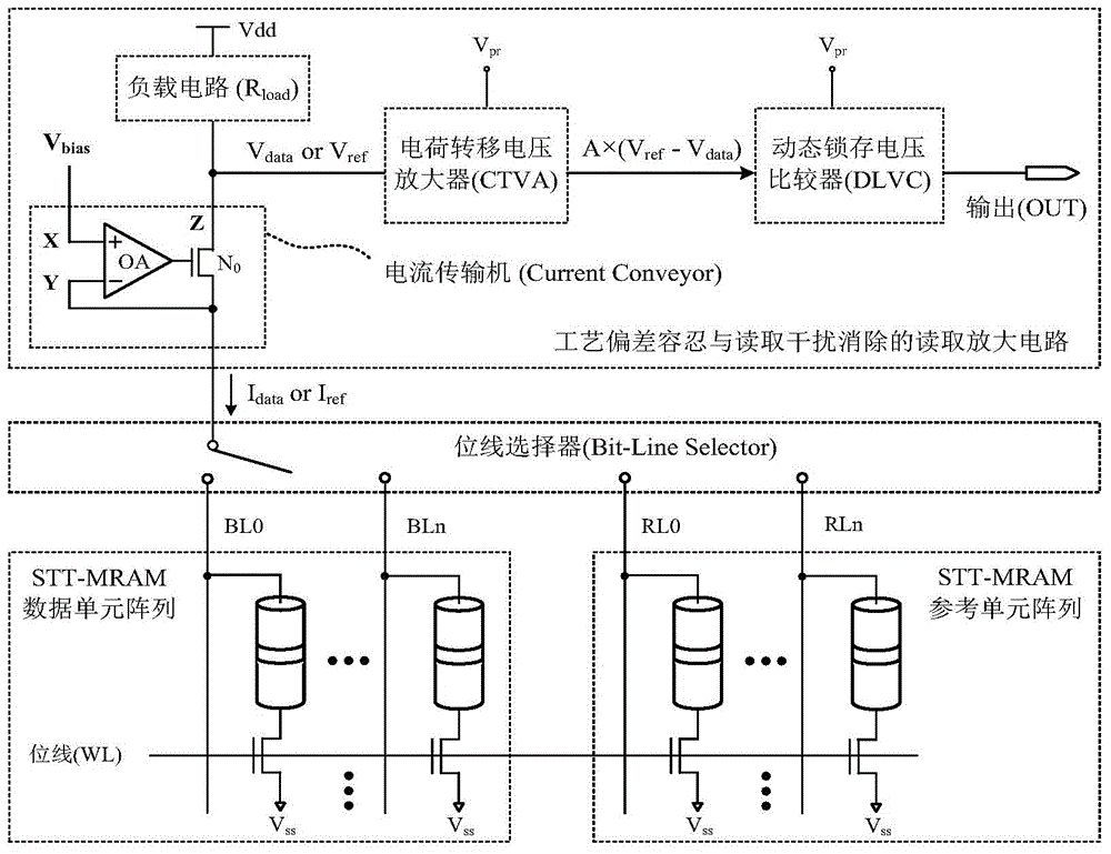
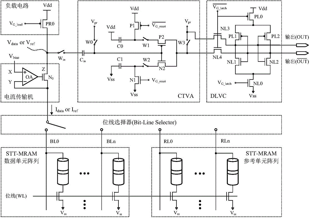
The invention provides a process deviation tolerating and reading interference eliminating reading amplifying circuit, which consists of a current conveyor, a load circuit, a charge transferring voltage amplifier and a dynamic latch voltage comparator, wherein one input end Y of the current conveyor is connected with an STT-MRAM (Spin Transfer Torque Magnetic Random Access Memory) data unit array to be read and an STT-MRAM reference unit array to be read through a bit line selector; the other input end X of the current conveyor is connected with an external bias voltage V<bias>; the output end Z of the current conveyor is simultaneously connected with the load circuit and the input end of the charge transferring voltage amplifier; the other end of the load circuit is connected with a power supply voltage source Vdd; the output end of the charge transferring voltage amplifier is connected with the input end of the dynamic latch voltage comparator; and the output end of the dynamic latch voltage comparator outputs final read binary data signals. The reading amplifying circuit provided by the invention has the advantages that the problem of conflict between the reading interference and the reading judging allowance in the STT-MRAM technology is solved, and the reading reliability of an STT-MRAM is improved.

Description

technical field [0001] The invention provides a read amplifier circuit with process deviation tolerance and read interference elimination, which belongs to the technical field of non-volatile STT-MRAM memory. Background technique [0002] In recent years, the new spin transfer torque magnetic random access memory STT-MRAM (Spin Transfer Torque Magnetic Random Access Memory) technology has been continuously developed, has become more and more mature, and has gradually begun to be used in actual industrial production. The basic storage unit of STT-MAM is mainly composed of a magnetic tunnel junction MTJ (Magnetic Tunneling Junction) and an N-type metal oxide semiconductor NMOS (N-Metal-Oxide-Semiconductor) transistor. Among them, MTJ is used for data storage, while NMOS transistor is used for access control of memory cells. MTJ is mainly composed of three layers of film, such as figure 1 As shown, that is, the upper and lower layers are ferromagnetic layers, and the middle i...

Claims


Application Information

Patent Timeline
Patent Type & Authority Applications(China)
IPC IPC(8): G11C7/06G11C16/26
Inventor 康旺郭玮赵巍胜张有光
Owner 致真存储(北京)科技有限公司
Why Eureka
Eureka Blog
Learn More