Method for ohmic contact between copper indium gallium diselenide and molybdenum and solar cell preparation method

An ohmic contact, copper indium gallium selenide technology, applied in circuits, electrical components, photovoltaic power generation, etc., can solve the problem of destroying the mechanical connection performance of CIGS thin film and Mo thin film, increasing the contact resistance between Mo thin film and CIGS thin film, and increasing the series resistance of CIGS battery. and other problems, to achieve the effect of saving industrial development, reducing additional processing, and avoiding uncontrollability

Inactive Publication Date: 2014-11-05
PEKING UNIV
View PDF5 Cites 4 Cited by
  • Summary
  • Abstract
  • Description
  • Claims
  • Application Information

AI Technical Summary

Problems solved by technology

However, even if a MoSe2 film is prepared on a Mo film, there may not be a good ohmic contact, and certain conditions need to be met, and this preparation method is complicated and difficult to control
Improper preparation process will increase the contact resistance between Mo th...

Method used


Image

  • Method for ohmic contact between copper indium gallium diselenide and molybdenum and solar cell preparation method
  • Method for ohmic contact between copper indium gallium diselenide and molybdenum and solar cell preparation method
  • Method for ohmic contact between copper indium gallium diselenide and molybdenum and solar cell preparation method

Examples


Embodiment Construction

[0030] The present invention will be further described through the embodiments below in conjunction with the accompanying drawings.

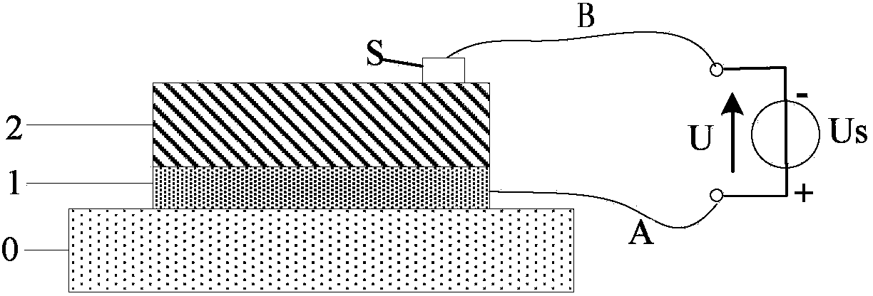
[0031] Such as figure 1 As shown, the method for changing the ohmic contact between copper indium gallium selenide and molybdenum in this embodiment includes the following steps:

[0032] 1) Prepare a 500nm Mo thin film 1 on a glass substrate 0 by sputtering;

[0033] 2) A 1.2 μm CIGS thin film 2 was prepared on the Mo thin film 1 by the selenization method after sputtering;

[0034] 3) Provide two electrode lines, one end of the first electrode line A is connected to the positive pole of the power supply, the other end is connected to the Mo film 1, one end of the second electrode line B is connected to the negative pole of the power supply Us, and the other end is connected to the scanning component S, the scanning component S is placed on the CIGS film 2, in this embodiment, the scanning component S uses a scanning slider;

[0035]4) Turn ...


PUM

PropertyMeasurementUnit
Widthaaaaaaaaaa

Abstract

The invention discloses a method for ohmic contact between copper indium gallium diselenide and molybdenum and a solar cell preparation method. After a CIGS thin film is formed on a Mo thin film, power voltage is applied between the CIGS thin film and the Mo thin film, a scanning assembly carries out two-dimensional scanning on the surface of the CIGS thin film, the contact-potential barrier between the Mo thin film and the CIGS thin film is broken through, internal resistance of the thin-film solar cell is reduced, and conditions are created for improving efficiency of the solar cell. According to the method for ohmic contact between copper indium gallium diselenide and molybdenum and the solar cell preparation method, through the voltage application mode, additional processing on the surface of the Mo thin film can be reduced, the number of procedures is reduced, uncontrollability caused by additional technologies is avoided, the implementation methods are quite simple, and input of subsequent industrial development is saved.

Description

technical field [0001] The invention relates to the preparation of thin-film solar cells, in particular to a method for changing the ohmic contact between copper indium gallium selenium and molybdenum and a method for preparing solar cells. Background technique [0002] Thin-film solar cells have become the main development direction of future batteries due to their low loss and high yield characteristics. Copper indium gallium selenide solar cells are one of the main development directions in thin film solar cells. Its structure includes from bottom to top: glass or flexible substrate, molybdenum Mo thin film, copper indium gallium selenide CIGS thin film, cadmium sulfide CdS thin film, zinc oxide ZnO thin film, aluminum-doped zinc oxide ZnO:Al thin film and surface electrode, among them, sulfide The contact resistance between the cadmium film to the zinc oxide film and between the zinc oxide film and the aluminum-doped zinc oxide film, because the material itself is well ...

Claims


Application Information

Patent Timeline
IPC IPC(8): H01L31/0224H01L31/18
CPCH01L31/022425H01L31/18Y02E10/50Y02P70/50
Inventor 焦飞赵夔陆真冀
Owner PEKING UNIV
Why Eureka
Try Eureka