GaN film growing on Zr substrate, preparation method and application

A thin film and substrate technology, which is applied in the field of GaN thin film grown on Zr substrate and its preparation, can solve the problems of unstable chemical properties of metal Zr substrate, affecting the quality of epitaxial thin film growth, difficulty in thin film epitaxy, etc., and achieves improved The effect of internal quantum efficiency, shortening nucleation time, and improving light extraction efficiency

Inactive Publication Date: 2014-11-05
SOUTH CHINA UNIV OF TECH
View PDF6 Cites 0 Cited by
  • Summary
  • Abstract
  • Description
  • Claims
  • Application Information

AI Technical Summary

Problems solved by technology

[0006] However, the metal Zr substrate is chemically unstable at high temperature. When the epitaxial temperature is higher than 700 °C, the interface reaction between the epitaxial nitride and the metal substrate will seriously affect the quality of the epitaxial film growth.
Pioneering researcher and well-known scientist Akasaki et al. have tried to apply traditional MOCVD or MBE technology to directly epitaxially grow nitrides on substrate materials with variable chemical properties. difficulty

Method used


Image

  • GaN film growing on Zr substrate, preparation method and application
  • GaN film growing on Zr substrate, preparation method and application
  • GaN film growing on Zr substrate, preparation method and application

Examples


Embodiment 1

[0034] The preparation method of the GaN thin film grown on the Zr substrate of the present implementation comprises the following steps:

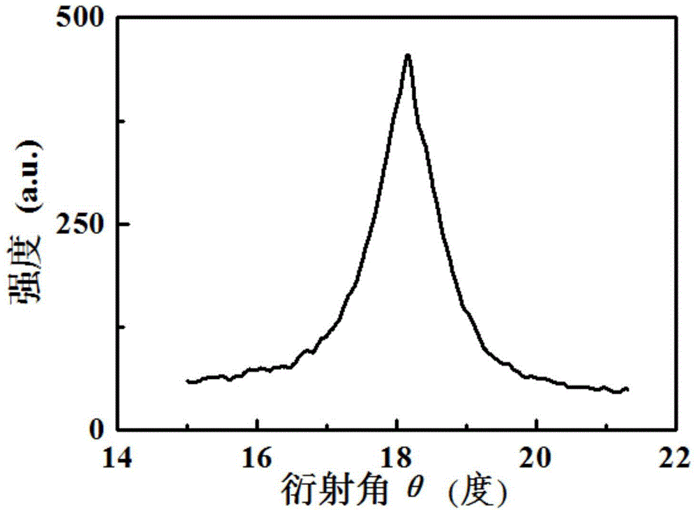
[0035] (1) Selection of the substrate and its crystal orientation: the epitaxial substrate adopts the (0001) plane of the Zr substrate as the epitaxial plane, and the selected crystal epitaxial orientation relationship: GaN(0001) / / Zr(0001).

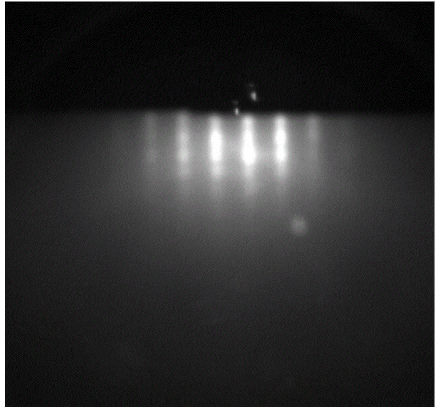
[0036] (2) Epitaxial growth of GaN film: the substrate temperature was raised to 500°C, and the reaction chamber pressure was 4×10 -5 Torr, Ⅴ / Ⅲ ratio is 50, growth rate is 0.6ML / s; energy consumption is 3.0J / cm 2And a KrF excimer laser (λ=248nm, t=20ns) with a repetition rate of 30Hz ablates the Ga target material, and continuously feeds nitrogen plasma to epitaxially grow a 20nm GaN film on the substrate.

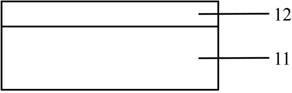
[0037] Such as figure 1 As shown, the GaN thin film grown on the Zr substrate prepared in this embodiment includes a Zr substrate 11 , a GaN thin film 12 , and the GaN thin film layer 12 is on t...

Embodiment 2

[0044] The preparation method of the GaN thin film grown on the Zr substrate of the present embodiment comprises the following steps:

[0045] (1) Selection of the substrate and its crystal orientation: the epitaxial substrate adopts the (0001) plane of the Zr substrate as the epitaxial plane, and the selected crystal epitaxial orientation relationship: GaN(0001) / / Zr(0001).

[0046] (2) Epitaxial growth of GaN film: the substrate temperature was raised to 700°C, and the reaction chamber pressure was 3×10 -5 Torr, Ⅴ / Ⅲ ratio is 60, growth rate is 0.4ML / s; energy consumption is 3.0J / cm 2 And a KrF excimer laser (λ=248nm, t=20ns) with a repetition rate of 30Hz ablates the Ga target material, and continuously injects nitrogen plasma to epitaxially grow a 100nm GaN film on the substrate.

[0047] The performance of the GaN thin film grown on the Zr substrate prepared in this embodiment is similar to that of Embodiment 1, and will not be repeated here.


PUM

PropertyMeasurementUnit
thicknessaaaaaaaaaa
thicknessaaaaaaaaaa
thicknessaaaaaaaaaa

Abstract

The invention discloses a GaN film growing on a Zr substrate. The GaN film sequentially comprises the Zr substrate and a GaN film part from the bottom up, wherein the GaN film part is a GaN film part growing at 500-700 DEG C. The invention further discloses a preparation method and an application of the GaN film growing on the Zr substrate. The GaN film growing on the Zr substrate has the advantages of low dislocation density and good crystal quality; the Zr substrate is easy to obtain and low in price; and the production cost can be lowered.

Description

technical field [0001] The invention relates to a GaN thin film and a preparation method, in particular to a GaN thin film grown on a Zr substrate, a preparation method and an application. Background technique [0002] Light-emitting diode (LED), as a new type of solid-state lighting source and green light source, has outstanding features such as small size, low power consumption, environmental protection, long service life, high brightness, low heat and colorful, and is widely used in outdoor lighting, commercial lighting and decoration Engineering and other fields have a wide range of applications. At present, under the background of the increasingly serious problem of global warming, saving energy and reducing greenhouse gas emissions has become an important issue faced by the whole world. A low-carbon economy based on low energy consumption, low pollution, and low emissions will become an important direction of economic development. In the field of lighting, the applic...

Claims


Application Information

Patent Timeline
Patent Type & Authority Applications(China)
IPC IPC(8): H01L33/02H01L33/32
CPCH01L33/12H01L33/007H01L33/16
Inventor 李国强王文樑杨为家刘作莲林云昊周仕忠钱慧荣
Owner SOUTH CHINA UNIV OF TECH
Why Eureka
Try Eureka