Organic light-emitting diode array substrate and display device
A technology for light-emitting diodes and array substrates, which is applied to light-emitting materials, organic semiconductor devices, chemical instruments and methods, etc., can solve the problems of low light-emitting efficiency and complicated preparation equipment, and achieves the advantages of improving light-emitting efficiency, simplifying preparation equipment and reducing costs. Effect
- Summary
- Abstract
- Description
- Claims
- Application Information
AI Technical Summary
Problems solved by technology
Method used
Image

Examples
Embodiment 1
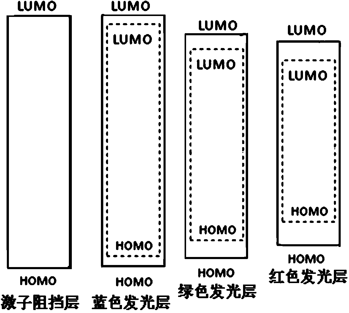
[0026] This embodiment provides an organic light emitting diode array substrate, which includes a plurality of organic light emitting diodes. The organic light emitting diodes include sequentially arranged anodes, light emitting layers, and cathodes. The light emitting layers are divided into multiple colors, and are composed of host materials and doped The composition of the guest material in the host material; and the organic light emitting diode further includes:
[0027] The exciton blocking layer disposed between the anode and the light-emitting layer and in contact with the light-emitting layer is composed of a host material of the light-emitting layer that has the largest highest occupied molecular orbital energy level and three-line state energy level.
[0028] The exciton blocking layer exists in the organic light emitting diode array substrate of this embodiment, so it can increase the probability of mutual quenching of triplet excitons and improve the luminous effic...
Embodiment 2
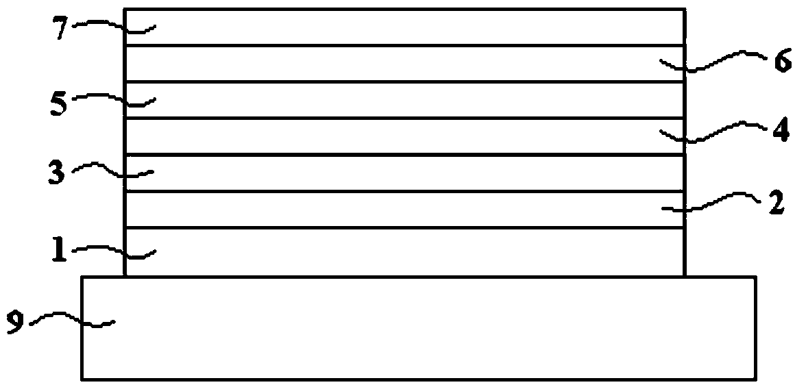
[0046] Such as figure 2 , image 3 As shown, the present embodiment provides an organic light emitting diode array substrate.
[0047] The organic light emitting diode array substrate includes a plurality of sub-pixels, and each sub-pixel is provided with an organic light-emitting diode; meanwhile, the sub-pixels are divided into three colors: red, green, and blue, that is, the organic light-emitting diodes in the sub-pixels are also divided into Red, green, blue three colors.
[0048] Specifically, such as figure 2 As shown, the organic light emitting diode is arranged on the substrate 9 (usually made of glass), and in the direction away from the substrate 9, it includes in turn:
[0049] (1) The anode 1 is made of transparent indium tin oxide (ITO) material and has a thickness of 130 nm.
[0050] (2) Hole injection layer 2, which is composed of 4,4′,4″-tris(N-3-methylphenyl-N-phenylamino)triphenylamine (m-MTDATA, HOMO energy level 5.1eV, LUMO energy level 2.0eV) and a...
Embodiment 3
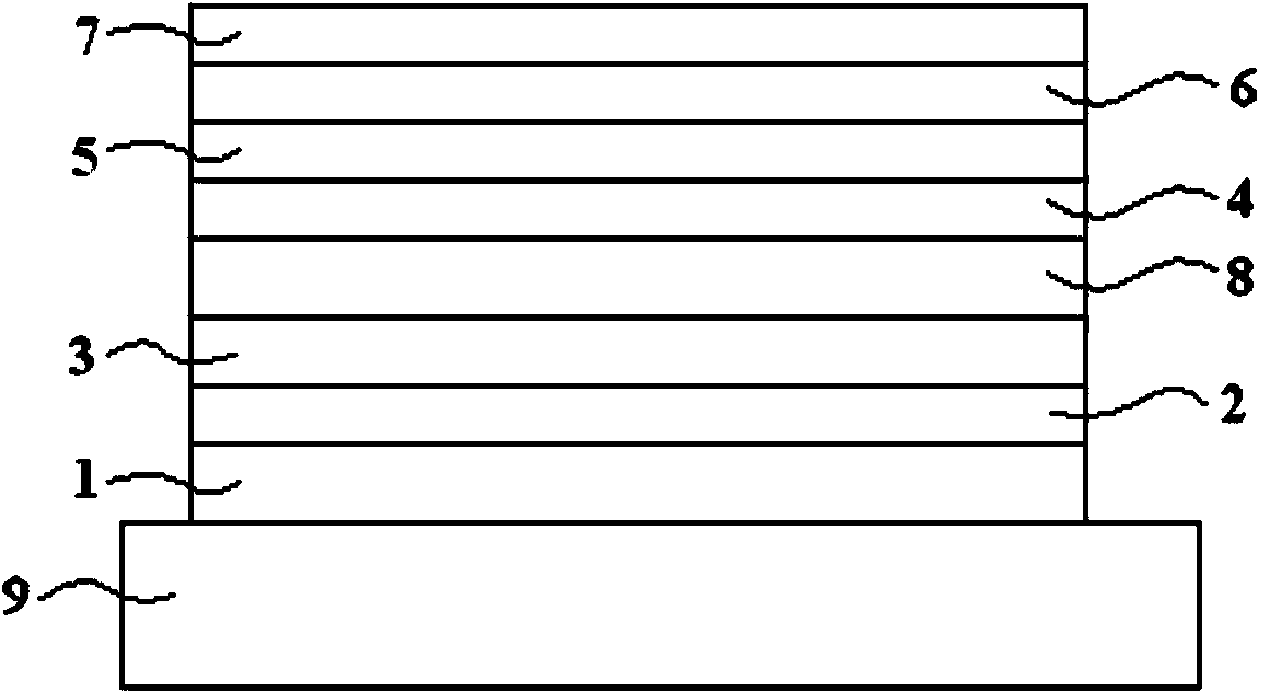
[0068] Such as figure 2 As shown, the present embodiment provides an organic light emitting diode array substrate.
[0069] The organic light emitting diode array substrate includes a plurality of sub-pixels, and each sub-pixel is provided with an organic light-emitting diode; meanwhile, the sub-pixels are divided into three colors: red, green, and blue, that is, the organic light-emitting diodes in the sub-pixels are also divided into Red, green, blue three colors.
[0070] Specifically, such as figure 2 As shown, each organic light emitting diode is arranged on a substrate 9 (usually made of glass), and in a direction away from the substrate 9, the organic light emitting diodes include in turn:
[0071] (1) The anode 1 is made of transparent indium tin oxide material with a thickness of 15 nm; and a metal reflective layer (such as a silver reflective layer) is provided on the side of the anode close to the substrate 9 .
[0072] The reason why the reflective layer is pr...
PUM
| Property | Measurement | Unit |
|---|---|---|
| Thickness | aaaaa | aaaaa |
| Thickness | aaaaa | aaaaa |
| Thickness | aaaaa | aaaaa |
Abstract
Description
Claims
Application Information
 - R&D
- Intellectual Property
- Life Sciences
- Materials
- Tech Scout
- Unparalleled Data Quality
- Higher Quality Content
- 60% Fewer Hallucinations
Browse by: Latest US Patents, China's latest patents, Technical Efficacy Thesaurus, Application Domain, Technology Topic, Popular Technical Reports.
© 2025 PatSnap. All rights reserved.Legal|Privacy policy|Modern Slavery Act Transparency Statement|Sitemap|About US| Contact US: help@patsnap.com