Reversed-polarity AlGaInP-based light-emitting diode and manufacturing method thereof

A technology of light-emitting diodes and manufacturing methods, which is applied in the field of optoelectronics, can solve problems affecting product quality and genuine product rate, poor metal layer adhesion, device voltage increase, etc., to improve quality and yield, improve adhesion and integrity, The effect of the integrity of the electrode structure

Active Publication Date: 2014-11-26
YANGZHOU CHANGELIGHT
View PDF3 Cites 25 Cited by
  • Summary
  • Abstract
  • Description
  • Claims
  • Application Information

AI Technical Summary

Problems solved by technology

Due to the dense and smooth surface of the epitaxially grown n-type GaAs ohmic contact layer, the adhesion to the metal layer is not good. In addition, when the chemical solution wet-etches the n-AlGaInP roughening layer, there is a serious problem of lateral undercutting. The edge of the extended electrode is in a suspended state. Under the action of external stress, it is easy to cause defects and peeling off of the extended electrode and the n-GaAs contact layer, which destroys the normal current extension, causes the voltage of the device to increase, and the brightness to decrease, which seriously affects the quality and quality of the product. Genuine rate

Method used


Image

  • Reversed-polarity AlGaInP-based light-emitting diode and manufacturing method thereof
  • Reversed-polarity AlGaInP-based light-emitting diode and manufacturing method thereof
  • Reversed-polarity AlGaInP-based light-emitting diode and manufacturing method thereof

Examples


Embodiment Construction

[0025] The present invention will be further described below in conjunction with the accompanying drawings and embodiments.

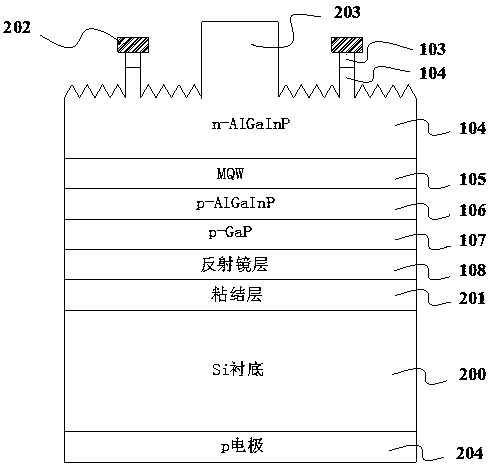
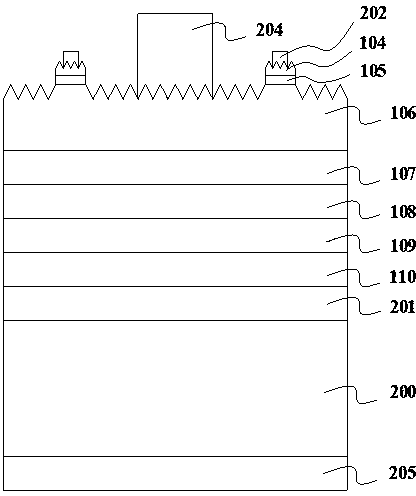
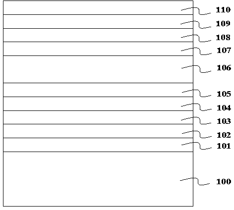
[0026] like figure 2 As shown, the present invention uses a Si substrate 200 as a permanent substrate, and has two main surfaces, upper and lower. Metal Au or Ag is used as the bonding layer 201 to form on its upper surface. The mirror layer 110 is formed on the bonding layer 201, and its material is a SiO2 / Ag double-layer structure; the p-GaP window layer 109 is formed on the mirror layer 110; the p-AlGaInP confinement layer 108 is formed on the p-GaP window On the layer 109; the multi-quantum well (MQW) active layer 107 is formed on the p-AlGaInP confinement layer 108, and its material is AlGaInP; the n-AlGaInP confinement layer 106 is formed on the multi-quantum well (MQW) active layer 107 On; the n-GaAs ohmic contact layer 105 is formed on the n-AlGaInP confinement layer 106, its thickness is preferably 300 Angstroms, and the doping concentratio...


PUM

PropertyMeasurementUnit
thicknessaaaaaaaaaa
thicknessaaaaaaaaaa
thicknessaaaaaaaaaa

Abstract

The invention discloses a reversed-polarity AlGaInP-based light-emitting diode and a manufacturing method thereof and belongs to the technical field of photoelectron. The method includes the following steps: firstly manufacturing a light-emitting-diode epitaxial wafer and manufacturing a holophote structure layer on the epitaxial wafer; bonding the epitaxial wafer provided with the holophote structure layer and a permanent substrate through a metal bonding layer; coarsening the surface of a first coarsening layer through removal of a temporary substrate, a buffer layer, a barrier layer and an n-type gallium arsenide layer; manufacturing patterned extending electrodes on the first coarsening layer and the n-type gallium arsenide ohmic contact layer; using a mask to protect existing patterned extending electrodes and removing the first coarsening layer and the n-type gallium arsenide ohmic contact layer, which are outside a mask protective layer and coarsening a second coarsening layer; and forming a main electrode on the second coarsening layer. The method uses a coarsening epitaxial layer structure and mask protection to improve adhesiveness and integrity of the electrodes and the epitaxial layer so that work voltage stability of a light-emitting device is ensured and product quality and yield are improved significantly.

Description

technical field [0001] The invention belongs to the technical field of optoelectronics, in particular to the manufacturing technology of reverse-polarity AlGaInP-based light-emitting diodes. Background technique [0002] High-brightness AlGaInP light-emitting diodes have been widely used in the field of high-efficiency solid-state lighting, such as display screens, automotive lights, backlight sources, traffic lights, landscape lighting, etc. Since the forbidden band width of the conventional GaAs substrate is narrower than that of AlGaInP, the photons emitted downward generated by the active region will be absorbed, resulting in a significant reduction in luminous efficiency. In order to prevent photons emitted downward from being absorbed and improve luminous efficiency, a GaP substrate with a wider bandgap than AlGaInP can be used to replace the GaAs substrate, but this process technology has the disadvantages of complex equipment, low yield, and high manufacturing cost. ...

Claims


Application Information

Patent Timeline
Patent Type & Authority Applications(China)
IPC IPC(8): H01L33/14H01L33/02H01L33/00
CPCH01L33/0066H01L33/10H01L33/22
Inventor 陈亮杨凯马祥柱白继锋陈宝李忠辉
Owner YANGZHOU CHANGELIGHT
Why Eureka
Try Eureka