
Method for manufacturing multilayer PCB in plate pressing mode

A technology of PCB board and manufacturing method, applied in the field of multi-layer PCB board press plate manufacturing, can solve the problems of layer and layer offset, PCBA failure, affecting the bonding force between PCB layers and layers, etc., to achieve the effect of fewer layers

Active Publication Date: 2014-11-26
GCI SCI & TECH
View PDF7 Cites 9 Cited by
  • Summary
  • Abstract
  • Description
  • Claims
  • Application Information

AI Technical Summary

Problems solved by technology

When the multi-layer thick bottom copper (≥3OZ) adopts one-step lamination, the lamination in the middle of the PCB multi-layer board is unevenly stressed due to the copper surface and the copper-free area, because the copper-free area needs to be filled with more resin. During the process, the copper-free area needs to be filled with resin. The pressure of the interval is lower than that of the copper surface, which is easy to produce resin voids, leaving serious hidden dangers for the subsequent inner layer short circuit and reflow soldering. Infiltrating the cavity and plating copper can cause a short circuit and cause the PCBA to fail
At the same time, after most of the resin is used to fill the copper-free area, the copper surface will be in direct contact with the glass cloth due to the lack of resin, which will affect the bonding force between PCB layers and layers.
However, when encountering a thick-bottomed copper core board with a thin inner layer substrate (0.1mm), the resin flow will cause layer-to-layer offset, which will also leave hidden dangers of internal short.

Method used


Image

  • Method for manufacturing multilayer PCB in plate pressing mode
  • Method for manufacturing multilayer PCB in plate pressing mode
  • Method for manufacturing multilayer PCB in plate pressing mode

Examples


Embodiment 1

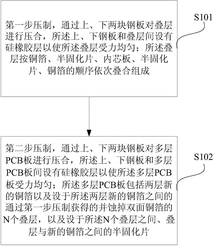
[0023] figure 1 The flow chart of the method for manufacturing a multi-layer PCB plate pressing plate provided by Embodiment 1 of the present invention, the specific steps include:

[0024] S101: the first step is pressing, the lamination is pressed by two upper and lower steel plates, and a silicon rubber layer is provided between the upper and lower steel plates and the lamination so that the lamination is evenly stressed; the lamination It is composed of copper foil, prepreg, inner core board, prepreg and copper foil in sequence;

[0025] S102: the second step is pressing, the multi-layer PCB board is pressed through the upper and lower two steel plates, and a silicon rubber layer is arranged between the upper and lower steel plates and the multi-layer PCB board so that the multi-layer PCB board is stressed Uniform; the multi-layer PCB board comprises two layers of new copper foils and N laminated layers obtained by pressing the first step and etching away the double-sided...

Embodiment 2

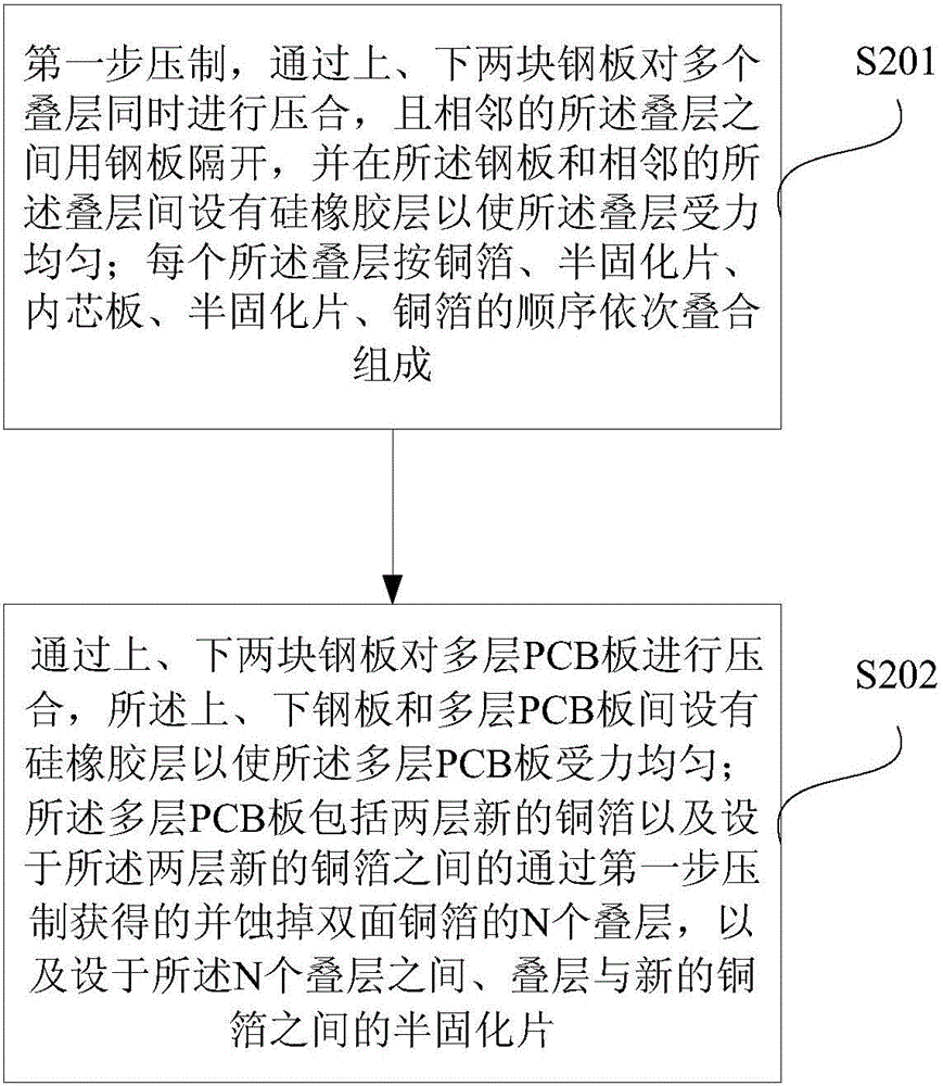
[0036] figure 2 The flow chart of the manufacturing method of the multi-layer PCB plate pressing plate provided by Embodiment 2 of the present invention, the specific steps include:

[0037] S201: The first step of pressing is to simultaneously press a plurality of laminations through the upper and lower steel plates, and the adjacent laminations are separated by steel plates, and between the steel plates and the adjacent A silicone rubber layer is provided between the laminations to make the laminations evenly stressed; each of the laminations is composed of copper foil, prepreg, inner core board, prepreg, and copper foil in sequence;

[0038] S202: the second step is pressing, the multi-layer PCB board is pressed through the upper and lower two steel plates, and a silicon rubber layer is arranged between the upper and lower steel plates and the multi-layer PCB board so that the multi-layer PCB board is stressed Uniform; the multi-layer PCB board comprises two layers of new...

Embodiment 3

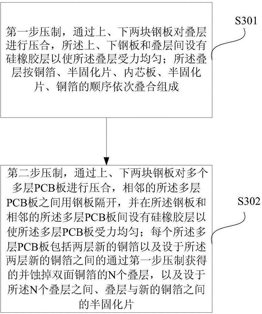
[0049] image 3 The flow chart of the method for manufacturing a multi-layer PCB board press plate provided by Embodiment 3 of the present invention, the specific steps include:

[0050] S301: the first step is pressing, the lamination is pressed by the upper and lower steel plates, and a silicon rubber layer is provided between the upper and lower steel plates and the lamination to make the lamination evenly stressed; the lamination It is composed of copper foil, prepreg, inner core board, prepreg and copper foil in sequence;

[0051] S302: In the second step of pressing, a plurality of multi-layer PCB boards are pressed together by upper and lower two steel plates, and the adjacent multi-layer PCB boards are separated by steel plates, and the steel plates and the adjacent multi-layer PCB boards are separated A silicone rubber layer is provided between the multilayer PCB boards so that the multilayer PCB boards are evenly stressed; each of the multilayer PCB boards includes ...


PUM

PropertyMeasurementUnit
Thicknessaaaaaaaaaa
Thicknessaaaaaaaaaa

Abstract

The invention discloses a method for manufacturing a multilayer PCB in a plate pressing mode. The method comprises the steps that plate pressing is conducted through two steps, wherein the first step of pressing is conducted, press fitting is conducted on stacked layers through an upper steel plate and a lower steel plate, silicone rubber layers are arranged between the upper steel plate and the stacked layers and between the lower steel plate and the stacked layers so that the stacked layers can be evenly stressed, and the stacked layers are formed by sequentially stacking copper foil, prepreg, an inner core plate, prepreg and copper foil; the second step of pressing is conducted, press fitting is conducted on the multilayer PCB through the upper steel plate and the lower steel plate, and silicone rubber layers are arranged between the upper steel plate and the multilayer PCB and between the lower steel plate and the multilayer PCB so that the multilayer PCB can be evenly stressed, and the multilayer PCB comprises two layers of new copper foil, the N stacked layers which are arranged between the two layers of new copper foil and obtained through the first step of pressing with the double-face copper foil corroded, and prepreg arranged between the N stacked layers and between the stacked layers and the new copper foil. By means of the method for manufacturing the multilayer PCB in the plate pressing mode, the phenomena of interlayer cavities, insufficient interlayer combining force and layer deviation can be effectively controlled.

Description

technical field [0001] The invention relates to the field of circuit board manufacturing, in particular to a method for manufacturing a multilayer PCB pressing board. Background technique [0002] In the electronics industry, the AC / DC power supply market is usually one of the most stable markets, and it is widely used in computer networks, communication equipment, consumer electronics equipment, automotive industry and other fields. The development trend of AC / DC power supply makes the terminal products have more and more stringent requirements for printed circuit boards, especially for the current conduction capacity and carrying capacity of printed circuit boards. The thickness is getting thicker and thicker, and the thick copper printed circuit board that can provide high current and integrate power supply will gradually become a trend in the development of the printed circuit board industry in the future. [0003] At present, the circuit board manufacturing industry ad...

Claims


Application Information

Patent Timeline
IPC IPC(8): H05K3/46
Inventor 张韬
Owner GCI SCI & TECH
Learn More